One of the main objectives of our work is to analyse electronic and optical properties of semiconductor and metal surfaces. To measure in situ (during growth) instead of ex situ (after growth) optical methods such as Reflectance Anisotropy Spectroscopy (RAS), Spectroscopic Ellipsometry (SE), Raman Spectroscopy and Magneto-Optical Kerr Spectroscopy (MOKE) are used. Complementary information is also gained in Ultra-High Vacuum (UHV) by Scanning Tunneling Microscopy (STM), Photo-Emission Spectroscopy (PES), Low Energy Electron Diffraction (LEED), and Auger Electron Spectroscopy (AES).
This combination makes it possible to monitor the surface in situ with optical tools. On the other hand, Raman, RAS and SE spectra are being influenced by other parameters (morphology, composition, doping) that provide information UHV based tools cannot obtain easily. Also the interaction between local structure (STM) and log range order (LEED) is part of these investigation. The newest addition are MOKE (analysis of magnetic layers), Infrared Spectroscopy (FTIR), and true in-situ Atomic Force Microscopy (AFM) is in preparation.
The aim is to understand growth of new materials like InGaN or ferromagenetic semiconductors. On the other hand for III-V semiconductors like GaInAsP to control layer properties like roughness, to control size and density of quantuum dots by a feedback from the in-situ measurements to the growth process.
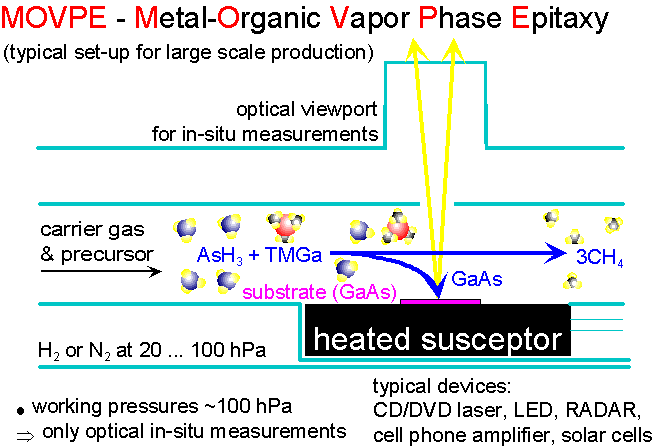
Schematic setup of an in-situ MOVPE reactor.
Contact:
- Wolfgang Richter (General Coordination)
- Markus Pristovsek, Florian Poser, Stefan Weeke (III-V MOVPE)
- Torsten Schmidtling, Massimo Drago (Nitride)
- Christian Kaspari, Eugen Speiser, Bert Rähmer (in-situ technology)
Collaboration:
- University of Jena (Prof. Bechstedt): total energy ab-initio calculations of optical properties and reconstructions
- Fritz-Haber-Institut of the Max-Planck-Gesellschaft Berlin with the theory department on DFT calculations of III-V growth related topics
Research projects:
- SFB 290: Special Research Center "Thin Metal Films" (Properties of magnetic layers)
- Collaborative research center Sfb 296: Investigations of the growth of low dimensional semiconductor structures
- In situ process control during fabrication of nanostructures and monolayers (NanOp research network)