|
|
Books
Semiconductor Nanophotonics - Materials, Models, and Devices
Editors: M. Kneissl, A. Knorr, S. Reitzenstein, A. Hoffmann
|
Chapter 5: Optical and Structural Properties of Nitride Based Nanostructures
F. Bertram, C. Berger, J. Christen, H. Eisele, L. A. Th. Greif, A. Hoffmann, J. Maultzsch, M. Müller, E. Poliani, G. Schmidt, P. Veit, and M. R. Wagner
Advanced characterization methods with nanoscale resolution are powerful tools in order to overcome the continuing challenges in the optimization of nitride semiconductor nanostructures for more efficient nanophotonic devices in the UV and green spectral range. This chapter is devoted to the study of optical, electronic, and structural properties of these nitride based nanostructures. In the first part, we discuss several state-of-the-art nanoscale characterization techniques including scanning transmission electronmicroscopy cathodoluminescence (STEMCL), tip-enhanced Raman spectroscopy (TERS), micro-photoluminescence (?PL), X-ray diffraction (XRD), and scanning tunneling microscopy and spectroscopy (STM/STS). This selection of complementary microscopic and spectroscopic techniques provides unique insights into a multitude of nanostructure properties such as charge carrier excitation, relaxation, diffusion, and recombination dynamics, vibrational and structural properties including strain, segregation, as well as clustering, and surface and interface morphology. In the second part, we apply and combine these techniques to obtain detailed information on nanoscale properties of nitride based micro-columns, quantum wires, and heterostructures.The study of these nitride nanostructures provides not only insight into device limitations, but also contributes to the fundamental understanding of structural and optical properties of III-nitride nanostructures.
Chapter 12: Nitride Microcavities and Single Quantum Dots for Classical and Non-classical Light Emitters
G. Schmidt, C. Berger, A. Dadgar, F. Bertram, P. Veit, S. Metzner, A. Strittmatter, J. Christen, S. T. Jagsch, M. R. Wagner, and A. Hoffmann
Microcavities with InGaN quantum wells or GaN-based quantum dots as active medium are building blocks of electrically-driven, low-threshold surfaceemitting lasers or single photon emitters in the visible-to-UV spectral range. In this chapter, we highlight essential developments in epitaxial growth techniques of such nitride-based microcavities and their active regions.Modern analytical techniques for structural and optical characterization of these complex heterostructures as presented in this chapter are essential to solve remaining challenges.
Springer Series in Solid State Science, Vol. 194 (2020)
1st Edition., 2020, XXIII, 556 p. 374 illus., 337 in color.
ISBN: 978-3-030-35655-2
|
|
|
Zinc Oxide: From Fundamental Properties Towards Novel Applications
C. F. Klingshirn, B. K. Meyer, A. Waag, A. Hoffmann, J. Geurts
Chapter 8: Influence of External Fields
M. R. Wagner and A. Hoffmann
|
This book gives a comprehensive review of the present state of the art in ZnO R+D, including growth, doping, lattice dynamics, electric magnetic and optical properties. The emphasis is on the electric and optical properties, because this is the area where novel applications may be expected with highest promise. The book highlights not only the most recent results but gives both an overview of past research and of the present status -- not avoiding critical and controversial discussions of various aspects such as band symmetries and laser processes. Intended to have long-lasting impact on ZnO R+D, this monograph addresses (post-)graduate students but also advanced scientists, who want to embark on ZnO research or are already involved, the present state of the art and assists them in avoiding duplication of old results (or mistakes).
The application of external fields provides a powerful tool to investigate a large variety of properties of excitons and exciton related processes. Within this chapter, we focus on the fundamental effects of static magnetic and strain fields on the optical properties of excitons in ZnO. The description is complemented by relevant examples. A general review of this topic can be found for constant fields in [Cho, Excitons, Topics in Current Physics, vol. 14 (Springer, Heidelberg, 1979)] and Hönerlage et al. [Physics Reports 124, 161 (1985)] and for modulation techniques in [Cardona, Modulation Spectroscopy (Academic, New York, 1969); Seraphin, Modulation Spectroscopy (North Holland, Amsterdam, 1973); Goldsmith, NATO Science Series II, Frontiers of Optical Spectroscopy, Vol. 168 (Springer Netherlands, 2005)].
Springer Series in Materials Science, Vol. 120 (2010)
1st Edition., 2010, XIII, 300 p. 200 illus., 100 in color.
ISBN: 978-3-642-10576-0
|

|
|
Publications
2018
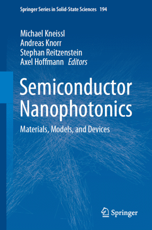
(80) Comparative study of the pressure dependence of optical-phonon transverse-effective charges and linewidths in wurtzite InN
J. S. Reparaz1, K. Pereira da Silva1,2, A. H. Romero3,4, J. Serrano5, M. R. Wagner6, G. Callsen6, S. J. Choi7, J. S. Speck7, and A. R. Goni1,8
1Institut de Ciència de Materials de Barcelona-CSIC, Esfera UAB, 08193, Bellaterra, Spain
2Fac. de Física, Univ. Fed. Do Pará, CEP 66075-110, Belém, PA, Brazil
3Physics Department, West Virginia University, Morgantown, USA
4Facultad de Ingeniería, Benemérita Universidad Autnoma de Puebla, 72570, Puebla, Pue., México
5Yachay Tech University, School of Physical Sciences and Nanotechnology, Urcuqu 100119, Ecuador
6Institut für Festkörperphysik, Technische Universität Berlin, Hardenbergstr. 36, 10623 Berlin, Germany
7Materials Department, University of California, Santa Barbara, CA 93106-5050, USA
8ICREA, Passeig Lluís Companys 23, 08010 Barcelona, Spain
|
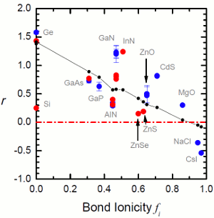
We investigate the hydrostatic pressure dependence of the zone center optical phonons of c-plane and a-plane wurtzite InN epilayers grown on GaN substrates. The longitudinal to transverse mode splitting for the A1 and E1 modes was found to increase with increasing pressure, whereas the associated transverse effective charge decreases for both modes as eT*(A1)=2.93-9.9x10⁻³ and eT*(E1)=2.80-10.6x10⁻³ P (in units of elementary charge and P in GPa). These observations are well in line with results for other II-VI, III-V, and group-IV semiconductor compounds as far as the relation between the magnitude and sign of the pressure derivative of eT* and the bond ionicity is concerned. As the latter increases so does |∂eT*/∂P| with a sign change from positive to negative for bond ionicities around fi=0.46 for compounds with anions belonging to the first row of the periodic table. A comparison of the results for InN and other nine tetrahedrally bonded compounds indicate that the pressure behavior of the transverse effective charge is mainly determined by the strength of the Pauli repulsion between cation valence electrons and those of the anion core. We also perform ab-initio calculations in order to address the origin of the observed increase in linewidth of the E2high mode which is found to arise from a pressure-induced increase in the rate of two-phonon decay processes. This broadening is associated with tuning into resonance of a steep edge in the two-phonon density of states around 460 cm-1 with the frequency of the E2high mode.
Physical Review B 98, 165204 (Oct. 16, 2018)
|
|
|
(79) Suppression of the quantum-confined Stark effect in polar nitride heterostructures
S. Schlichting1, G. M. O. Hönig2, J. Müßener3, P. Hille3, T. Grieb3, S. Westerkamp1, J. Teubert4, J. Schörmann4, M. R. Wagner1, A. Rosenauer3, M. Eickhoff3, A. Hoffmann1, and G. Callsen1,5
1Institut für Festkörperphysik, Technische Universität Berlin, Hardenbergstr. 36, 10623 Berlin, Germany
2Bundesanstalt für Materialforschung und -prüfung (BAM), 12200 Berlin, Germany
3Institut für Festkörperphysik, Universität Bremen, Otto-Hahn-Allee 1, 28359 Bremen, Germany
4I. Physikalisches Institut, Justus-Liebig Universität Giessen, Heinrich-Buff-Ring 16, 35392 Giessen, Germany
5Institute of Physics, École Polytechnique Fédérale de Lausanne (EPFL), CH-1015 Lausanne, Switzerland
|
Recently, we suggested an unconventional approach (the so-called Internal-Field-Guarded-Active-Region Design "IFGARD") for the elimination of the quantum-confined Stark effect in polar semiconductor heterostructures. The IFGARD based suppression of the Stark redshift on the order of electronvolt and spatial charge carrier separation is independent of the specific polar semiconductor material or the related growth procedures. In this work, we demonstrate by means of micro-photoluminescence techniques the successful tuning as well as the elimination of the quantum-confined Stark effect in strongly polar [000-1] wurtzite GaN/AlN nanodiscs as evidenced by a reduction of the exciton lifetimes by up to four orders of magnitude. Furthermore, the tapered geometry of the utilized nanowires (which embed the investigated IFGARD nanodiscs) facilitates the experimental differentiation between quantum confinement and Stark emission energy shifts. Due to the IFGARD, both effects become independently adaptable.
Communications Physics 1, 48 (Aug. 23, 2018)
|
|
|
(78) Auger recombination in AlGaN quantum wells for UV light-emitting diodes
F. Nippert1, M. T. Mazraehno2, M. J. Davies2, M. P. Hoffmann2, H.-J. Lugauer2, T. Kure1, M. Kneissl1, A. Hoffmann1, and M. R. Wagner1
1Institut für Festkörperphysik, Technische Universität Berlin, Hardenbergstr. 36, 10623 Berlin, Germany
2OSRAM Opto Semiconductors GmbH, Leibnizstr. 4, 93055 Regensburg, Germany
|
We show that the often observed effciency droop in AlGaN quantum well heterostructures is an internal carrier loss process, analogous to the InGaN system. We attribute this loss process to Auger recombination, with C=2.3x10⁻³⁰cm6s1; a similar value as found commonly in InGaN-based devices. As a result, the peak internal quantum efficiency (IQE) of our structures is limited to 66%. These values were obtained by resonant excitation (time-resolved) photoluminescence (PL), avoiding common error sources in IQE measurements. The existence of strong Auger recombination implies that simple methods for IQE determination, such as temperature-dependent PL may lead to erroneous values. Auger losses will have to be considered once the challenges regarding carrier injection are solved.
Applied Physics Letters 113, 071107 (Aug. 17, 2018)
|
|
|
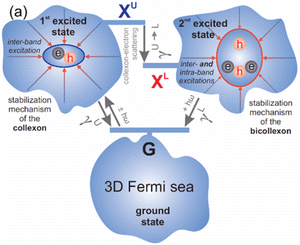
(77) Electronic excitations stabilised by a degenerate electron gas in semiconductors
C. Nenstiel1, G. Callsen1, F. Nippert1, T. Kure1, S. Schlichting1, N. Jankowski1, M. P. Hoffmann2, A. Dadgar2, S. Fritze2, A. Krost2, M. R. Wagner1, A. Hoffmann1, and F. Bechstedt3
1Institut für Festkörperphysik, Technische Universität Berlin, Hardenbergstraße 36, 10623 Berlin, Germany
2Institut für Experimentelle Physik, Fakultät für Naturwissenschaften, Otto-von-Guericke-Universität Magdeburg, Universitätsplatz 2, 39016 Magdeburg, Germany
3Institut für Festkörpertheorie und -optik, Friedrich-Schiller-Universität, Max-Wien-Platz 1, 07743 Jena, Germany
|
Excitons in semiconductors and insulators consist of fermionic subsystems, electrons and holes, whose attractive interaction facilitates bound quasiparticles with quasi-bosonic character. In the presence of a degenerate electron gas, such excitons dissociate due to free carrier screening. Despite their absence, we found pronounced emission traces in the below-band-edge region of bulk, germanium-doped GaN up to a temperature of 100?K, mimicking sharp spectral features at high free electron concentrations (3.4E19-8.9E19 cm-3). Our interpretation of the data suggests that a degenerate, three-dimensional electron gas stabilizes a novel class of quasiparticles, which we name collexons. These many-particle complexes are formed by exchange of electrons with the Fermi gas. The potential observation of collexons and their stabilization with rising doping concentration is enabled by high crystal quality due to the almost ideal substitution of host atoms with dopants.
Communication Physics 1, 38 (Jul. 26, 2018)
|
|
|
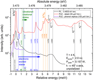
(76) Excited states of neutral donor bound excitons in GaN
G. Callsen1, T. Kure2, M. R. Wagner2, R. Butté1, and N. Grandjean1
1Institute of Physics, École Polytechnique Fédérale de Lausanne (EPFL), CH-1015 Lausanne, Switzerland
2Institut für Festkörperphysik, Technische Universität Berlin, Hardenbergstraße 36, 10623 Berlin, Germany
|
We investigate the excited states of a neutral donor bound exciton (D0X) in bulk GaN by means of high-resolution, polychromatic photoluminescence excitation (PLE) spectroscopy. The optically most prominent donor in our sample is silicon accompanied by only a minor contribution of oxygen?the key for an unambiguous assignment of excited states. Consequently, we can observe a multitude of Si0X-related excitation channels with linewidths down to 200 µeV. Two groups of excitation channels are identified, belonging either to rotational-vibrational or electronic excited states of the hole in the Si0X complex. Such identification is achieved by modeling the excited states based on the equations of motion for a Kratzer potential, taking into account the particularly large anisotropy of effective hole masses in GaN. Furthermore, several ground- and excited states of the exciton-polaritons and the dominant bound exciton are observed in the photoluminescence (PL) and PLE spectra, facilitating an estimate of the associated complex binding energies. Our data clearly show that great care must be taken if only PL spectra of D0X centers in GaN are analyzed. Every PL feature we observe at higher emission energies with regard to the Si0X ground state corresponds to an excited state. Hence, any unambiguous peak identification renders PLE spectra highly valuable, as important spectral features are obscured in common PL spectra. Here, GaN represents a particular case among the wide-bandgap, wurtzite semiconductors, as comparably low localization energies for common D0X centers are usually paired with large emission linewidths and the prominent optical signature of exciton-polaritons, making the sole analysis of PL spectra a challenging task.
Journal of Applied Physics 123, 215702 (Jun. 05, 2018)
|
|
|
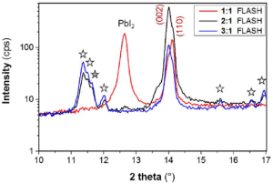
(75) Crystallisation behaviour of CH3NH3PbI3 films: The benefits of sub-second flash lamp annealing
R. Muydinov1, S. Seeger2, S. H. B. V. Kumar1, C. Klimm3, R. Kraehnert4, M. R. Wagner5, B. Szyszka1
1Institute of High-Frequency and Semiconductor System Technologies, Technical University Berlin, Einsteinufer 25, 10587 Berlin, Germany
2OUT (Optotransmitter-Umweltschutz-Technologie) e.V., Köpenicker Straße 325/201, 12555 Berlin, Germany
3Institute for Silicon Photovoltaics, Helmholtz-Zentrum Berlin, Kekuléstraße 5, 12489 Berlin, Germany
4Institute of Technical Chemistry, Technical University Berlin, Straße des 17. Juni 124, 10623 Berlin, Germany
5Institute of Solid State Physics, Technical University Berlin, Hardenbergstraße 36, 10623 Berlin, Germany
|
Crystallisation of the spin-coated hybrid perovskite films has some basic issues restraining the up-scaling of this technology. The reason consists in substantial chemical impact of the solvent during drying that lessens control of crystallisation and reproducibility. This current investigation proposes very fast crystallisation by means of a flash lamp to solve those issues. CH3NH3PbI3 films were prepared on glass and silicon substrates by spin-coating from N,N-dimethylformamide based solutions with various CH3NH3PbI3 to PbI2 ratios (1:1, 2:1 and 3:1). Thermal annealing of as-deposited films at 85°C, 120°C and 140°C was compared with the flash lamp annealing realised via sub-second high energy xenon light illumination from the uncoated glass side. Optimal light pulse length and energy density were found to be 2.7 ms and 8 J/cm2, respectively. According to our simulations based on the finite element model the perovskite layers underwent to a short-term heating to 350-425°C followed by cooling to 100°C within 3 ms. No decomposition of the perovskite was detected. Conversely its crystallinity according to the X-ray diffraction was prominently better as for thermally annealed films. Fourier-transform infrared spectroscopy revealed the effective elimination of the solvent from perovskite films by flash lamp annealing. High temperature was found to be crucial for the completeness of PbI2 reaction into the perovskite in stoichiometric films. High heating rate appeared to suppress the gel-like phase formation in super-stoichiometric films that helped to avoid the formation of pores. The flash lamp crystallised films revealed pore free microstructure with longitudinally extended grains regardless of the precursor ratio.
Thin Solid Films 653, 204 (Mar. 16, 2018)
|
|
|
(74) Optical Emission of GaN/AlN Quantum-Wires - The Role of Charge Transfer from the Nanowire Template
J. Müßener1,2, L. A. Th. Greif3, S. Kalinowski3, G. Callsen3, P. Hille1,2, J. Schörmann2, M. R. Wagner3, A. Schliwa3, S. Martí-Sánchez4, J. Arbiol4,5, A. Hoffmann3, and M. Eickhoff1,2
1Institut für Festkörperphysik, Universität Bremen, Otto-Hahn-Allee 1, 28359 Bremen, Germany
2I. Physikalisches Institut und Zentrum für Materialforschung, Justus-Liebig-Universität Gießen, Germany
3Institut für Festkörperphysik, Technische Universität Berlin, Hardenbergstr. 36, 10623 Berlin, Germany
4Catalan Institute of Nanoscience and Nanotechnology (ICN2), CSIC and BIST, Campus UAB, Bellaterra, 08193 Barcelona, Spain
5ICREA, Pg. Lluis Companys 23, 08010 Barcelona, Spain
|
We show that one-dimensional (1d) GaN quantum-wires (QWRs) exhibit intense and spectrally sharp emission lines. These QWRs are realized in an entirely self-assembled growth process by molecular beam epitaxy (MBE) on the side facets of GaN/AlN nanowire (NW) heterostructures. Time-integrated and time-resolved photoluminescence (PL) data in combination with numerical calculations allow the identification and assignment of the manifold emission features to three different spatial recombination centers within the NWs. The recombination processes in the QWRs are driven by efficient charge carrier transfer effects between the different optically active regions, providing high intense QWR luminescence despite their small volume. This is deduced by a fast rise time of the QWR PL, which is similar to the fast decay-time of adjacent carrier reservoirs. Such processes, feeding the ultra-narrow QWRs with carriers from the relatively large NWs, can be the key feature towards the realization of future QWR-based devices. While processing of single quantum structures with diameters in the nm range presents a serious obstacle with respect to their integration into electronic or photonic devices, the QWRs presented here can be analyzed and processed using existing techniques developed for single NWs.
Nanoscale 10, 5991 (Feb. 08, 2018)
|
|
|
2017
(73) Breakdown of Far-Field Raman Selection Rules by Light-Plasmon Coupling Demonstrated by Tip-Enhanced Raman Scattering
E. Poliani1, M. R. Wagner1, A. Vierck1, F. Herziger1, C. Nenstiel1, F. Gannott2, M. Schweiger2, S. Fritze3, A. Dadgar3, J. Zaumseil4, A. Krost3, A. Hoffmann1, and J. Maultzsch1,5
1Institut für Festkörperphysik, Technische Universität Berlin, 10623 Berlin, Germany
2Nanomaterials for Optoelectronics Group, Institute of Polymer Materials, Friedrich-Alexander-Universität Erlangen-Nürnberg, 91054 Erlangen, Germany
3Institut für Experimentelle Physik, Otto-von-Guericke-Universität Magdeburg, 39106 Magdeburg, Germany
4Physikalisch-Chemisches Institut Lehrstuhl für Angewandte Physikalische Chemie, Ruprecht-Karls-Universität Heidelberg, 69117 Heidelberg, Germany
5Department Physik, Friedrich-Alexander-Universität Erlangen-Nürnberg, 91054 Erlangen, Germany
|
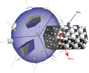
We present an experimental study on the near-field light-matter interaction by tip-enhanced Raman scattering (TERS) with polarized light in three different materials: germanium-doped gallium nitride (GaN), graphene, and carbon nanotubes. We investigate the dependence of the TERS signal on the incoming light polarization and on the sample carrier concentration, as well as the Raman selection rules in the near-field. We explain the experimental data with a tentative quantum mechanical interpretation, which takes into account the role of plasmon polaritons, and the associated evanescent field. The driving force for the breakdown of the classical Raman selection rules in TERS is caused by photon tunneling through the perturbation of the evanescent field, with the consequent polariton annihilation. Predictions based on this quantum mechanical approach are in good agreement with the experimental data, which are shown to be independent of incoming light polarization, leading to new Raman selection rules for TERS.
Journal of Physical Chemistry Letters (Oct. 24, 2017)
|
|
|
(72) Thermal transport in epitaxial Si1-xGex alloy nanowires with varying composition and morphology
A. El Sachat1, J. S. Reparaz2, J. Spiece3, M. I. Alonso2, A. R. Goni2, M. Garriga2, P. O. Vaccaro2,4, M. R. Wagner1, O. V. Kolosov3, C. M. Sotomayor Torres1,4, and F. Alzina1
1Catalan Institute of Nanoscience and Nanotechnology (ICN2), CSIC and BIST, Campus UAB, Bellaterra, 08193 Barcelona, Spain
2Institut de Ciència de Materials de Barcelona, ICMAB-CSIC, Campus Universitari de Bellaterra, E-08193 Bellaterra, Spain
3Physics Department, Lancaster University, Lancaster, UK
4ICREA Pg. Lluís Companys 23, 08010 Barcelona, Spain
|
We report on structural, compositional, and thermal characterization of self-assembled in-plane epitaxial Si1-xGex alloy nanowires grown by molecular beam epitaxy on Si (001) substrates. The thermal properties were studied by means of scanning thermal microscopy, while the microstructural characteristics, the spatial distribution of the elemental composition of the alloy nanowires and the sample surface were investigated by transmission electron microscopy and energy dispersive x-ray microanalysis. We provide new insights regarding the morphology of the in-plane nanostructures, their size-dependent gradient chemical composition, and the formation of a 5 nm thick wetting layer on the Si substrate surface. In addition, we directly probe heat transfer between a heated scanning probe sensor and Si1-xGex alloy nanowires of different morphological characteristics and we quantify their thermal resistance variations. We correlate the variations of the thermal signal to the dependence of the heat spreading with the cross-sectional geometry of the nanowires using finite element method simulations. With this method we determine the thermal conductivity of the nanowires with values in the range of 2-3 Wm-1K-1. These results provide valuable information in growth processes and show the great capability of the scanning thermal mi-croscopy technique in ambient environment for nanoscale thermal studies, otherwise not possible using conventional tech-niques.
Nanotechnology 28, 505704 (Oct. 19, 2017)
|
|
|
(71) Modification of thermal conductivity and phonon dispersion relation by means of phononic crystals
M. Sledzinska1, A. El Sachat1,2, J. S. Reparaz1, M. R. Wagner1, F. Alzina1, and C. M. Sotomayor Torres1,3
1Catalan Institute of Nanoscience and Nanotechnology (ICN2), CSIC and BIST, Campus UAB, Bellaterra, 08193 Barcelona, Spain
2Dept. of Physics, Universitat Autnoma de Barcelona, Campus UAB, Bellaterra, 08193 Barcelona, Spain
3Institució Catalana de Recerca i Estudis Avançats (ICREA), 08010 Barcelona, Spain
|
Heat conduction in silicon can be effectively reduced by means of periodic patterning of free-standing membranes. In this work we show a straightforward method for fabrication of free-standing phononic crystals based on thin silicon membranes. We use the contactless two-laser Raman thermometry method to measure thermal conductivity of the hexagonal phononic crystals. The aim of the study is to understand and control the behaviour of phonons in phononic crystals, with the target of minimizing the thermal conductivity. In particular, we are interested in the influence of the surface-to-volume ratio on the thermal conductivity.
IEEE Therminic 23, 01 (Sept. 27, 2017)
|
|
|
(70) Thermal conductivity and air-mediated losses in periodic porous silicon membranes at high temperatures
B. Graczykowski1,2,3, A. El Sachat1,4, J. S. Reparaz1,8, M. Sledzinska1, M. R. Wagner1,9, E. Chavez-Angel1, S. Volz5,6, Y. Wu5, F. Alzina1, and C. M. Sotomayor Torres1,7
1Catalan Institute of Nanoscience and Nanotechnology (ICN2), CSIC and BIST, Campus UAB, Bellaterra, 08193 Barcelona, Spain
2NanoBioMedical Centre, Adam Mickiewicz University, ul. Umultowska 85, PL-61614 Poznan, Poland
3Max Planck Institute for Polymer Research, Ackermannweg 10, 55218 Mainz, Germany
4Department of Physics, Universitat Autonoma de Barcelona, Campus UAB, Bellaterra, 08193 Barcelona, Spain
5Laboratoire dEnergetique Moleculaire et Macroscopique, Combustion, CNRS, CentraleSupelec, Grande Voie des Vignes, 92295 Chatenay-Malabry, France
6Laboratory for Integrated Micro-Mechatronics Systems, CNRS UMI2820, Institute of Industrial Science, University of Tokyo, 4-6-1 Komaba, Meguro-ku, Tokyo 153-8505, Japan
7ICREA Pg. Lluís Companys 23, 08010 Barcelona, Spain
8Institut de Ciència de Materials de Barcelona, ICMAB-CSIC, Campus Universitari de Bellaterra, E-08193 Bellaterra, Spain
9Institute of Solid State Physics, Technische Universität Berlin, Hardenbergstr. 36 10623 Berlin, Germany
|
Heat conduction in silicon can be effectively engineered by means of sub-micrometre porous thin free-standing membranes. Tunable thermal properties make these structures good candidates for integrated heat management units such as waste heat recovery, rectification or efficient heat dissipation. However, possible applications require detailed thermal characterisation at high temperatures which, up to now, has been an experimental challenge. In this work we use the contactless two-laser Raman thermometry to study heat dissipation in periodic porous membranes at high temperatures via lattice conduction and air-mediated losses. We find the reduction of the thermal conductivity and its temperature dependence closely correlated with the structure feature size. On the basis of two-phonon Raman spectra, we attribute this behaviour to diffuse (incoherent) phonon-boundary scattering. Furthermore, we investigate and quantify the heat dissipation via natural air-mediated cooling, which can be tuned by engineering the porosity.
Nature Communications 8, 415 (Mar. 24, 2017)
|
|
|
(69) Influence of carbon doping and hydrogen co-doping on acceptor related optical transitions in ZnO nanowires
F. Mohammadbeigi1, T. Kure2, G. Callsen2, E. Senthil Kumar1,3, M. R. Wagner2, A. Hoffmann2, and S. P. Watkins1
1Physics Department, Simon Fraser University, Burnaby, BC, Canada
2Institut für Festkörperphysik, Technische Universität Berlin, Hardenbergstraße 36, 10623 Berlin, Germany
3SRM Research Institute, Department of Physics and Nanotechnology, India
|
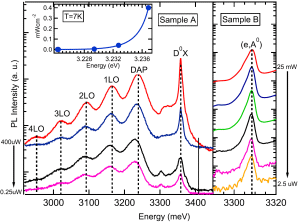
ZnO nanowires grown by metalorganic vapor phase epitaxy in the presence of carbon tetrachloride and hydrogen show two distinct low temperature photoluminescence (PL) bands at 3.237 and 3.309 eV. The band at 3.237 eV is most pronounced in samples grown in the presence of carbon tetrachloride, and is shown to be due to donor-acceptor pair (DAP) emission, based on intensity-dependent and time-resolved PL measurements. An acceptor binding energy of 181 ± 5 meV was inferred from these measurements. We attribute the acceptor in this DAP to the incorporation of nitrogen due to interaction between the carbon and nitrogen precursors. The addition of hydrogen in the presence of CCl4 results in a large enhancement of the carbon related shallow donor bound exciton PL, and the appearance of a strong band at 3.309 eV (e-A0) which is consistent with a free-to-bound transition, most likely (e-A0) as argued by previous works. The (e-A0) designation is based on detailed lineshape analysis as a function of temperature, together with time-resolved PL measurements. Based on this model, an acceptor binding energy for the 3.309 eV band of 133 ± 5 meV was determined, confirming and supporting previous reports.
Semiconductor Science and Technology 32, 045017 (Mar. 24, 2017)
|
|
|
2016
(68) Polarity in GaN and ZnO: theory, measurement, growth, and devices
J. Zúñiga-Pérez1, V. Consonni1,2, L. Lymperakis3, X. Kong4, A. Trampert4, S. Fernández-Garrido4, O. Brandt4, H. Renevier2, S. Keller5, K. Hestroffer5, M. R. Wagner6, J. S. Reparaz6, F. Akyol7, S. Rajan7, S. Rennesson8, T. Palacios8, and G. Feuillet9
1CRHEA, CNRS, F-06560 Valbonne, France
2Université Grenoble Alpes, CNRS, LMGP, F-38016, Grenoble, France
3Computational Materials Design Department, Max-Planck-Institut für Eisenforschung, Max-Planck.Str. 1, 40237 Düsseldorf, Germany
4Paul-Drude-Institut für Festkörperelektronik, Hausvogteiplatz 5-7, 10117 Berlin, Germany
5Electrical and Computer Engineering Department, University of California, Santa Barbara, CA 93106, USA
6Institute of Solid State Physics, Technische Universität Berlin, Hardenbergstr. 36, 10623 Berlin, Germany
7Electrical and Computer Engineering Department, The Ohio State University, Columbus, OH 43210, USA
8Microsystems Technology Laboratory, Department of Electrical Engineering and Computer Science, Massachusetts Institute of Technology, Cambridge, MA 02139, USA.
9Université Grenoble Alpes, CEA, LETI, F-38054, Grenoble, France
|
The polar nature of the wurtzite crystalline structure of GaN and ZnO results in the existence of a spontaneous electric polarization within these materials and their associated alloys (Ga,Al,In)N and (Zn,Mg,Cd)O. The polarity has also important consequences on the stability of the different crystallographic surfaces, and this becomes especially important when considering epitaxial growth. Furthermore, the internal polarization fields may adversely affect the properties of optoelectronic devices, but is also used as a potential advantage for advanced electronic devices. In this article, polarity-related issues in GaN and ZnO are reviewed, going from theoretical considerations to electronic and optoelectronic devices, through thin film and nanostructure growth. The necessary theoretical background is first introduced and the stability of the cation and anion polarity surfaces is discussed. For assessing the polarity one has to make use of specific characterization methods, which are described in detail. Subsequently, the nucleation and growth mechanisms of thin films and nanostructures, including nanowires, are presented, reviewing the specific growth conditions that allow controlling the polarity of such objects. Eventually, the demonstrated and/or expected effects of polarity on the properties and performances of optoelectronic and electronic devices are reported. The present review is intended to yield an in-depth view of some of the hot topics related to polarity in GaN and ZnO, a fast growing subject over the last decade.
Applied Physics Reviews 3, 041303 (Nov. 15, 2016)
|
|
|
(67) Temperature-dependent recombination coefficients in InGaN light-emitting diodes: Hole localization, Auger processes, and the green gap
F. Nippert1, S. Y. Karpov2, G. Callsen1, B. Galler3, T. Kure1, C. Nenstiel1, M. R. Wagner1, M. Straßburg3, H.-J. Lugauer3, and A. Hoffmann1
1Institut für Festkörperphysik, Technische Universität Berlin, Hardenbergstraße 36, 10623 Berlin, Germany
2STR Group-Soft-Impact Ltd., P.O. Box 83, 27 Engels av., 194156 St. Petersburg, Russia
3OSRAM Opto Semiconductors GmbH, Leibnizstraße 4, 93055 Regensburg, Germany
|
We obtain temperature-dependent recombination coefficients by measuring the quantum efficiency and differential carrier lifetimes in the state-of-the-art InGaN light-emitting diodes. This allows us to gain insight into the physical processes limiting the quantum efficiency of such devices. In the green spectral range, the efficiency deteriorates, which we assign to a combination of diminishing electron-hole wave function overlap and enhanced Auger processes, while a significant reduction in material quality with increased In content can be precluded. Here, we analyze and quantify the entire balance of all loss mechanisms and highlight the particular role of hole localization.
Applied Physics Letters 109, 161103 (Oct. 18, 2016)
|
|
|
(66) Two-Dimensional Phononic Crystals: Disorder Matters
M. R. Wagner1, B. Graczykowski1, J. S. Reparaz1, A. El Sachat1,2, M. Sledzinska1, F. Alzina1, and C. M. Sotomayor-Torres1,3
1Catalan Institute of Nanoscience and Nanotechnology (ICN2), CSIC and The Barcelona Institute of Science and Technology, Campus UAB, Bellaterra, 08193 Barcelona, Spain
2Dept. of Physics, UAB, 08193 Bellaterra (Barcelona), Spain
3Institució Catalana de Recerca i Estudis Avançats (ICREA), 08010 Barcelona, Spain
|
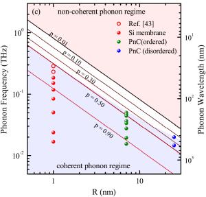
The design and fabrication of phononic crystals (PnCs) hold the key to control the propagation of heat and sound at the nanoscale. However, there is a lack of experimental studies addressing the impact of order/disorder on the phononic properties of PnCs. Here, we present a comparative investigation of the influence of disorder on the hypersonic and thermal properties of two-dimensional PnCs. PnCs of ordered and disordered lattices are fabricated of circular holes with equal filling fractions in free-standing Si membranes. Ultrafast pump and probe spectroscopy (asynchronous optical sampling) and Raman thermometry based on a novel two-laser approach are used to study the phononic properties in the gigahertz (GHz) and terahertz (THz) regime, respectively. Finite element method simulations of the phonon dispersion relation and three-dimensional displacement fields furthermore enable the unique identification of the different hypersonic vibrations. The increase of surface roughness and the introduction of short-range disorder are shown to modify the phonon dispersion and phonon coherence in the hypersonic (GHz) range without affecting the room-temperature thermal conductivity. On the basis of these findings, we suggest a criteria for predicting phonon coherence as a function of roughness and disorder.
Nano Letters 16, 5661 (Aug. 31, 2016)
|
|
|
(65) Measurement and modeling of the effective thermal conductivity of sintered silver pastes
J. Ordonez-Miranda1,2, M. Hermens3, I. Nikitin4, V. G. Kouznetsova3, O. van de Sluis3,5, M. Abo Ras6,7, J. S. Reparaz8, M. R. Wagner8, M. Sledzinska8, J. Gomis-Bresco8, C. M. Sotomayor Torres8,9, B. Wunderle10, S. Volz1
1Laboratoire d'Energétique Moléculaire et Macroscopique, Combustion, CNRS, Centrale Supelec, Grande Voie des Vignes, 92295 Chatenay-Malabry, France
2Institut Prime, CNRS, Université de Poitiers, ISAE-ENSMA, F-86962, Futuroscope, Chasseneuil, France
3Department of Mechanical Engineering, Eindhoven University of Technology, Eindhoven, The Netherlands
4INFINEON Technologies AG, Wernerwerkstrasse 2, 93049, Regensburg, Germany
5Philips Research Laboratories, High Tech Campus 34, 5656 AE, Eindhoven, The Netherlands
6Berliner Nanotest und Design GmbH, Berlin, Germany
7Fraunhofer Institute for Electronic Nano Systems ENAS, Chemnitz, Germany
8Catalan Institute of Nanoscience and Nanotechnology (ICN2), CSIC and The Barcelona Institute of Science and Technology, Campus UAB, Bellaterra, 08193 Barcelona, Spain
9ICREA, Catalan Institute for Research and Advanced Studies, 08010 Barcelona, Spain
10Technical University of Chemnitz, Reichenhainer Str. 70, 09126, Chemnitz, Germany
|
The effective thermal conductivity of sintered porous pastes of silver is modeled through two theoretical methods and measured by means of three experimental techniques. The first model is based on the differential effective medium theory and provides a simple analytical description considering the air pores like ellipsoidal voids of different sizes, while the second one arises from the analysis of the scanning-electron-microscope images of the paste cross-sections through the finite element method. The predictions of both approaches are consistent with each other and show that the reduction of the thermal conductivity of porous pastes can be minimized with spherical pores and maximized with pancake-shaped ones, which are the most efficient to block the thermal conducting pathways. A thermal conductivity of 151.6 W/m K is numerically determined for a sintered silver sample with 22% of porosity. This thermal conductivity agrees quite well with the one measured by the Lateral Thermal Interface Material Analysis for a suspended sample and matches, within an experimental uncertainty smaller than 16%, with the values obtained by means of Raman thermometry and the 3u technique, for two samples buried in a silicon chip. The consistence between our theoretical and experimental results demonstrates the good predictive performance of our theoretical models to describe the thermal behavior of porous thermal interface materials and to guide their engineering with a desired thermal conductivity.
International Journal of Thermal Sciences 108, 185 (May 09, 2016)
|
|
|
(64) Catalytically doped semiconductors for chemical gas sensing: Aerogel-like aluminum-containing zinc oxide materials prepared in the gas phase
K. Hagedorn1,4, W. Li2, Q. Liang3, S. Dilger1, M. Noebels3, M. R. Wagner5, J. S. Reparaz5, A. Dollinger3, J. Schmedt auf der Günne2, T. Dekorsy3, L. Schmidt-Mende3, and S. Polarz1
1Department of Chemistry, University of Konstanz, Universitätsstrasse 10, 78574 Konstanz, Germany
2Department of Chemistry and Biology, University of Siegen, Adolf-Reichwein-Strasse 2, 57076 Siegen, Germany
3Department of Physics, University of Konstanz, Universitätsstrasse 10, 78574 Konstanz, Germany
4EMPA-Material Science and Technology, Ueberlandstrasse 129, 8600 Dübendorf, Switzerland
5Catalan Institute of Nanoscience and Nanotechnology (ICN2), CSIC and The Barcelona Institute of Science and Technology, Campus UAB, Bellaterra, 08193 Barcelona, Spain
|
Atmospheric contamination with organic compounds is undesired in industry and in society because of odor nuisance or potential toxicity. Resistive gas sensors made of semiconducting metal oxides are effective in the detection of gases even at low concentration. Major drawbacks are low selectivity and
missing sensitivity toward a targeted compound. Acetaldehyde is selected due to its high relevance in chemical industry and its toxic character. Considering the similarity between gas-sensing and heterogeneous catalysis (surface reactions, activity, selectivity), it is tempting to transfer concepts. A question of importance is how doping and the resulting change in electronic properties of a metal-oxide support with semiconducting properties alters reactivity of the surfaces and the functionality in gas-sensing and in heterogeneous catalysis. A gas-phase synthesis method is employed for aerogel-like zinc oxide materials with a defi ned content of aluminum (n-doping), which were then used for the assembly of gas sensors. It is shown that only Al-doped ZnO represents an effective sensor material that is sensitive down to very low concentrations (<350 ppb). The advance in properties relates to a catalytic effect for the doped semiconductor nanomaterial.
Advanced Functional Materials 26, 3424 (Apr. 08, 2016)
|
|
|
(63) Spatially controlled growth of highly crystalline ZnO nanowires by an inkjet-printing catalyst-free method
F. Güell1, P. R. Martínez-Alanis1, S. Khachadorian2, R. R. Zamani1, A. Franke2, A. Hoffmann2, M. R. Wagner3, and G. Santana4
1Departament dElectrònica, Universitat de Barcelona, C/Martí i Franquès 1, 08028 Barcelona, Catalunya, Spain
2Institut für Festkörperphysik, Technische Universität, Hardenbergstr. 36, 10623, Berlin, Germany
3Catalan Institute of Nanoscience and Nanotechnology (ICN2), CSIC and The Barcelona Institute of Science and Technology, Campus UAB, Bellaterra, 08193 Barcelona, Spain
4Instituto de Investigaciones en Materiales, Universidad Nacional Autónoma de México, Ciudad Universitaria, 04510, D.F., México
|
High-density arrays of uniform ZnO nanowires with a high-crystal quality have been synthesized by a catalyst-free vapor-transport method. First, a thin ZnO film was deposited on a Si substrate as nucleation layer for the ZnO nanowires. Second, spatially selective and mask-less growth of ZnO nanowires was achieved using inkjet-printed patterned islands as the nucleation sites on a SiO2/Si substrate. Raman scattering and low temperature photoluminescence measurements were applied to characterize the structural and optical properties of the ZnO nanowires. The results reveal negligible amounts of strain and defects in the mask-less ZnO nanowires as compared to the ones grown on the ZnO thin film, which underlines the potential of the inkjet-printing approach for the growth of high-crystal quality ZnO nanowires.
Materials Research Express 03, 025010 (Feb. 11, 2016)
|
|
|
(62) Nanophononics: State of the art and perspectives
S. Volz1, J. Ordonez-Miranda1, A. Shchepetov2, M. Prunnila2, J. Ahopelto2, T. Pezeril3, G. Vaudel3, V. Gusev4, P. Ruello3, E. M. Weig5, M. Schubert5, M. Hettich5, M. Grossman5, T. Dekorsy5, F. Alzina6, B. Graczykowsky6, E. Chavez-Angel6, J. S. Reparaz6, M. R. Wagner6, C. M. Sotomayor-Torres6,7, S. Xiong8, S. Neogi9, and D. Donadio8,10,11,12
1Laboratoire d'Energétique Moléculaire et Macroscopique, Combustion, CNRS, Centrale Supelec, Grande Voie des Vignes, 92295 Chatenay-Malabry, France
2VTT Technical Research Centre of Finland, P.O. Box 1000, 02044 VTT, Espoo, Finland
3Institut des Molécules et Matériaux du Mans, UMR CNRS 6283, Université du Maine, 72085 Le Mans, France
4Laboratoire d'Acoustique UMR CNRS 6613, Université du Maine, 72085 Le Mans, France
5Department of Physics, University of Konstanz, Universitätsstr. 10, 78457 Konstanz, Germany
6Catalan Institute of Nanoscience and Nanotechnology (ICN2), CSIC and The Barcelona Institute of Science and Technology, Campus UAB, Bellaterra, 08193 Barcelona, Spain
7ICREA, Catalan Institute for Research and Advanced Studies, 08010 Barcelona, Spain
8Max Planck Institute for Polymer Research, Ackermannweg 10, 55128, Mainz, Germany
9Department of Aerospace Engineering Sciences, University of Colorado Boulder, Boulder, Colorado 80309, USA
10Department of Chemistry, University of California Davis, One Shields Ave. Davis, CA, 95616
11Ikerbasque, Basque Foundation for Science, Bilbao, Spain
12Donostia International Physics Center, Paseo M. de Lardizabal 4, 20018, San Sebastian, Spain
|
Understanding and controlling vibrations in condensed matter is emerging as an essential necessity both at fundamental level and for the development of a broad variety of technological applications. Intelligent design of the band structure and transport properties of phonons at the nanoscale and of their
interactions with electrons and photons impact the efficiency of nanoelectronic systems and thermoelectric materials, permit the exploration of quantum phenomena with micro- and nanoscale resonators, and provide new tools for spectroscopy and imaging. In this colloquium we assess the state of the art of nanophononics, describing the recent achievements and the open challenges in nanoscale heat transport, coherent phonon generation and exploitation, and in nano- and optomechanics. We also underline the links among the diverse communities involved in the study of nanoscale phonons and the common goals and opportunities.
European Journal of Physics B 89, 15 (Jan. 20, 2016)
|
|
|
2015
(61) A single-source precursor route to anisotropic halogen-doped zinc oxide particles as a promising candidate for new transparent conducting oxide materials
D. Lehr1, M. R. Wagner2, J. Flock1, J. S. Reparaz2, C. M. Sotomayor Torres2,3, A. Klaiber1, T. Dekorsy1, and S. Polarz1
1University of Konstanz, Universitaetsstr. 10, 78464 Konstanz, Germany
2ICN2 - Catalan Institute of Nanoscience and Nanotechnology, Campus UAB, 08193 Bellaterra (Barcelona), Spain
3Catalan Institute of Research and Advanced Studies (ICREA), Barcelona 08010, Spain
|
Numerous applications in optoelectronics require electrically conducting materials with high optical transparency over the entire visible light range. A solid solution of indium oxide and substantial amounts of tin oxide for electronic doping (ITO) is currently the most prominent example for the class of so-called TCOs (transparent conducting oxides). Due to the limited, natural occurrence of indium and its steadily increasing price, it is highly desired to identify materials alternatives containing highly abundant chemical elements. The doping of other metal oxides (e.g., zinc oxide, ZnO) is a promising approach, but two problems can be identified. Phase separation might occur at the required high concentration of the doping element, and for successful electronic modification it is mandatory that the introduced heteroelement occupies a defined position in the lattice of the host material. In the case of ZnO, most attention has been attributed so far to n-doping via substitution of Zn2+ by other metals (e.g., Al3+). Here, we present first steps towards n-doped ZnO-based TCO materials via substitution in the anion lattice (O2- versus halogenides). A special approach is presented, using novel single-source precursors containing a potential excerpt of the target lattice 'HalZn·Zn3O3' preorganized on the molecular scale (Hal = I, Br, Cl). We report about the synthesis of the precursors, their transformation into halogene-containing ZnO materials, and finally structural, optical and electronic properties are investigated using a combination of techniques including FT-Raman, low-T photoluminescence, impedance and THz spectroscopies.
Beilstein Journal of Nanotechnology 6, 2161 (Nov. 18, 2015)
|
|
|
(60) Nanoparticle shape anisotropy and photoluminescence properties: Europium containing ZnO as a Model Case
M. Gerigk1, P. Ehrenreich1, M. R. Wagner2, I. Wimmer1, J. S. Reparaz2, C. M. Sotomayor Torres2,3, L. Schmidt-Mende1, and S. Polarz1
1University of Konstanz, Universitaetsstr. 10, 78464 Konstanz, Germany
2ICN2 - Catalan Institute of Nanoscience and Nanotechnology, Campus UAB, 08193 Bellaterra (Barcelona), Spain
3Catalan Institute of Research and Advanced Studies (ICREA), Barcelona 08010, Spain
|
The precise control over electronic and optical properties of semiconductor (SC) materials is pivotal for a number of important applications like in optoelectronics, photocatalysis or in medicine. It is well known that the incorporation of heteroelements (doping as a classical case) is a powerful method for adjusting and enhancing the functionality of semiconductors. Independent from that, there already has been a tremendous progress regarding the synthesis of differently sized and shaped SC nanoparticles, and quantum-size effects are well documented experimentally and theoretically. Whereas size and shape control of nanoparticles work fairly well for the pure compounds, the presence of a heteroelement is problematic because the impurities interfere strongly with bottom up approaches applied for the synthesis of such particles, and effects are even stronger, when the heteroelement is aimed to be incorporated into the target lattice for chemical doping. Therefore, realizing coincident shape control of nanoparticle colloids and their doping still pose major difficulties. Due to a special mechanism of the emulsion based synthesis method presented here, involving a gelation of emulsion droplets prior to crystallization of shape-anisotropic ZnO nanoparticles, heteroelements can be effectively entrapped inside the lattice. Different nanocrystal shapes such as nanorods, -prisms, -plates, and -spheres can be obtained, determined by the use of certain emulsification agents. The degree of morphologic alterations depends on the type of incorporated heteroelement Mn+, concentration, and it seems that some shapes are more tolerant against doping than others. Focus was then set on the incorporation of Eu3+ inside the ZnO particles, and it was shown that nanocrystal shape and aspect ratios could be adjusted while maintaining a fixed dopant level. Special PL properties could be observed implying energy transfer from ZnO excited near its band-gap (3.3 eV) to the Eu3+ states mediated by defect luminescence of the nanoparticles. Indications for an influence of shape on photoluminescence (PL) properties were found. Finally, rod-like Eu@ZnO colloids were used as tracers to investigate their uptake into biological samples like HeLa cells. The PL was sufficient for identifying green and red emission under visible light excitation.
Nanoscale 7, 16969 (Sept. 19, 2015)
|
|
|
(59) Tuning thermal transport in ultrathin silicon membranes by surface nanoscale engineering
S. Neogi1, J. S. Reparaz2, L. F. C. Pereira3, B. Graczykowski2, M. R. Wagner2, M. Sledzinska2, A. Shchepetov4, M. Prunnila4, J. Ahopelto4, C. M. Sotomayor-Torres2,5, and D. Donadio1
1Max Planck Institute for Polymer Research, Ackermannweg 10, 55128 Mainz, Germany
2ICN2 - Catalan Institute of Nanoscience and Nanotechnology, Campus UAB, 08193 Bellaterra (Barcelona), Spain
3Departamento de Fisica Teorica e Experimental, Universidade Federal do Rio Grande do Norte, Natal 59078-900, Brazil
4VTT Technical Research Centre of Finland, P.O. Box 1000, FI-02044 VTT, Espoo, Finland
5Catalan Institute of Research and Advanced Studies (ICREA), Barcelona 08010, Spain
|
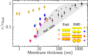
A detailed understanding of the connections of fabrication and processing to structural and thermal properties of low-dimensional nanostructures is essential to design materials and devices for phononics, nanoscale thermal management, and thermoelectric applications. Silicon provides an ideal platform to study the relations between structure and heat transport since its thermal conductivity can be tuned over 2 orders of magnitude by nanostructuring. Combining realistic atomistic modeling and experiments, we unravel the origin of the thermal conductivity reduction in ultrathin suspended silicon membranes, down to a thickness of 4 nm. Heat transport is mostly controlled by surface scattering: rough layers of native oxide at surfaces limit the mean free path of thermal phonons below 100 nm. Removing the oxide layers by chemical processing allows us to tune the thermal conductivity over 1 order of magnitude. Our results guide materials design for future phononic applications, setting the length scale at which nanostructuring affects thermal phonons most effectively.
ACS Nano 9, 3820 (Mar. 31, 2015)
|
|
|
(58) Optical and mechanical properties of nanofibrillated cellulose: towards a robust platform for next-generation green technologies
C. D. Simão1, J. S. Reparaz1, M. R. Wagner1, B. Graczykowski1, M. Kreuzer1, Y. B. Ruiz-Blanco1,2, Y. García1, J.-M. Malho3, A. R. Goñi4,5, J. Ahopelto3, C. M. Sotomayor Torres1,5
1ICN2 - Catalan Institute of Nanoscience and Nanotechnology, Campus UAB, 08193 Bellaterra (Barcelona), Spain
2Unit of Computer-Aided Molecular Biosilico Discovery and Bioinformatic Research (CAMD-BIR Unit), Faculty of Chemistry-
Pharmacy. Universidad Central Marta Abreu de Las Villas, Santa Clara, 54830, Villa Clara, Cuba
3VTT Technical Research Centre of Finland, P.O. Box 1000, FI-02044 VTT, Espoo, Finland
4Institut de Ciencia de Materials de Barcelona, ICMAB-CSIC, Barcelona, Spain
5Catalan Institute of Research and Advanced Studies (ICREA), Barcelona 08010, Spain
|
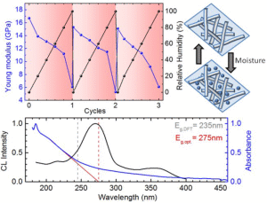
Nanofibrillated cellulose, a polymer that can be obtained from one of the most abundant biopolymers in Nature, is being increasingly explored due to its outstanding properties for packaging and device applications. Still, open challenges in engineering its intrinsic properties remain to address. To elucidate the optical and mechanical stability of nanofibrillated cellulose as a standalone platform, herein we report on three main findings: i) for the first time an experimental determination of the optical band gap of nanofibrillated cellulose, important for future modelling purposes, based on the onset of the optical band gap of the nanofibrillated cellulose film at Eg = 275 nm (4.5 eV), obtained using absorption and cathodoluminescence measurements. In addition, comparing this result with ab-initio calculations of the electronic structure the exciton binding energy is estimated to be Eex = 800 meV; ii) Hydrostatic pressure experiments revealed that nanofibrillated cellulose is structurally stable at least up to 1.2 GPa; iii) Surface elastic properties with repeatability better than 5% were observed under moisture cycles with changes of the Young modulus as large as 65%. The results obtained show the precise determination of significant properties as elastic properties and interactions that are compared with similar works and, moreover, demonstrate that nanofibrillated cellulose properties can be reversibly controlled, supporting the extended potential of nanofibrillated cellulose as a robust platform for green-technology applications.
Carbohydrate Polymers 126, 40 (Mar. 21, 2015)
|
|
|
(57) Phonon dispersion in hypersonic two-dimensional phononic crystal membranes
B. Graczykowski1, M. Sledzinska1, F. Alzina1, J. Gomis-Bresco1, J. S. Reparaz1, M. R. Wagner1, and C. M. Sotomayor Torres1,2
1ICN2 - Institut Catala de Nanociencia i Nanotecnologia, Campus UAB, 08193 Bellaterra (Barcelona), Spain
2Institució Catalana de Recerca i Estudis Avançats (ICREA), 08010 Barcelona, Spain
|
We investigate experimentally and theoretically the acoustic phonon propagation in two-dimensional phononic crystal membranes. Solid-air and solid-solid phononic crystals were made of square lattices of holes and Au pillars in and on 250 nm thick single crystalline Si membrane, respectively. The hypersonic phonon dispersion was investigated using Brillouin light scattering. Volume reduction (holes) or mass loading (pillars) accompanied with second-order periodicity and local resonances are shown to significantly modify the propagation of thermally activated GHz phonons. We use numerical modeling based on the finite element method to analyze the experimental results and determine polarization, symmetry, or three-dimensional localization of observed modes.
Physical Review B 91, 075414 (Feb. 13, 2015)
|
|
|
2014
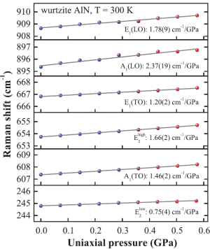
(56) Phonon pressure coefficients and deformation potentials of wurtzite AlN determined by uniaxial pressure-dependent Raman measurements
G. Callsen1, M. R. Wagner1, J. S. Reparaz1, F. Nippert1, T. Kure1, S. Kalinowski1, A. Hoffmann1, M. J. Ford2, M. R. Phillips2, R. F. Dalmau3, R. Schlesser3, R. Collazo4, and Z. Sitar4
1 Institute of Solid State Physics, Technische Universität Berlin, Hardenbergstr. 36, 10623 Berlin, Germany
2 Department of Physics and Advanced Materials, University of Technology Sydney, P.O. Box 123, Broadway, NSW 2007, Australia
3 HexaTech, Inc., 991 Aviation Pkwy, Morrisville, North Carolina 27560, USA
4 Material Science and Engineering, North Carolina State University, Raleigh, North Carolina, USA
|
We studied bulk crystals of wurtzite AlN by means of uniaxial pressure-dependent Raman measurements. As a result, we derive the phonon pressure coefficients and deformation potentials for all zone center optical phonon modes. For the A1 and E1 modes, we further experimentally determined the uniaxial pressure dependence of their longitudinal opticaltransverse optical (LO-TO) splittings. Our experimental approach delivers new insight into the large variance among previously reported phonon deformation potentials, which are predominantly based on heteroepitaxial growth of AlN and the ball-on-ring technique. Additionally, the measured phonon pressure coefficients are compared to their theoretical counterparts obtained by density functional theory implemented in the SIESTA package. Generally, we observe a good agreement between the calculated and measured phonon pressure coefficients but some particular Raman modes exhibit significant discrepancies similar to the case of wurtzite GaN and ZnO, clearly motivating the presented uniaxial pressure-dependent Raman measurements on bulk AlN crystals.
Physical Review B 90, 205206 (Nov. 07, 2014)
|
|
|
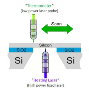
(55) A novel contactless technique for thermal conductivity determination: Two-Laser Raman Thermometry
J. S. Reparaz1, E. Chavez-Angel1,2, M. R. Wagner1, B. Graczykowski1, J. Gomis-Bresco1, F. Alzina1, and C. M. Sotomayor-Torres1,3
1 ICN2 - Institut Catala de Nanociencia i Nanotecnologia, Campus UAB, 08193 Bellaterra (Barcelona), Spain
2 Dept. of Physics, UAB, 08193 Bellaterra (Barcelona), Spain
3 Institució Catalana de Recerca i Estudis Avançats (ICREA), 08010 Barcelona, Spain
|
We present an extension of the method for thermal characterisation named Raman Thermometry that relaxes the assumption of boundary conditions by spatially resolving the thermal field. The technique is contact-less and suitable to study nanoscale systems unattainable to other by other more invasive thermal characterisation techniques.
IEEE Therminic 20, 01 (Sept. 24, 2014)
|
|
|
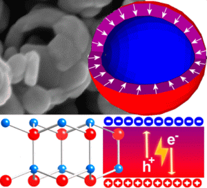
(54) Nanoarchitecture Effects on Persistent Room Temperature Photoconductivity and Thermal Conductivity in Ceramic Semiconductors: Mesoporous, Yolk-Shell, and Hollow ZnO Spheres
S. Dilger1, M. Wessig1, M. R. Wagner2, J. S. Reparaz2, C. M. Sotomayor Torres2,3, L. Qijun1, T. Dekorsy1, and S. Polarz1
1University of Konstanz, Universitätsstr. 10, 78457 Konstanz, Germany
2ICN2 - Institut Catala de Nanociencia i Nanotecnologia, Campus UAB, 08193 Bellaterra (Barcelona), Spain
3Institució Catalana de Recerca i Estudis Avançats (ICREA), 08010 Barcelona, Spain
|
Whereas size effects have been investigated extensively and are largely understood, it is significantly more challenging to elucidate how functional properties of semiconductors can be altered and ultimately be improved by a hierarchical nanoarchitecture. For semiconductor applications, such as in photovoltaics or photocatalysis, it is of great importance to learn how to avoid the recombination of photogenerated charge carriers and how to enhance their lifetime. A gas-phase synthesis method is explored, which enables the generation of spherical zinc oxide nanostructures with compact, mesoporous, a special type of core?shell, so-called yolk-shell, or hollow character. The particles with hollow character exhibit an extraordinarily long persistence of photogenerated charge carriers. It is demonstrated that the presence of the ZnO shell and its special orientation with respect to the polar character of the wurtzite lattice represent deciding factors. After photoexcitation, electrons and holes migrate to opposite sides of the interfaces, where they are stabilized. Moreover, photoluminescence thermometry was used to determine the thermal conductivity of the samples, which is lowered by a factor of 100 compared with bulk ZnO. The thermal conductivity of this type of nanostructure is found to be only 10 times larger than that of air, and this points toward potential applications as thermoelectrics.
Crystal Growth and Design 14, 4593 (Jul. 30, 2014)
|
|
|
(53) Dependence on pressure of the refractive indices of wurtzite ZnO, GaN and
AlN
A. R. Goni1,2, F. Käß3, J. S. Reparaz2,4, M. I. Alonso2, M. Garriga2, G. Callsen3, M. R. Wagner3,4, A. Hoffmann3, and Z. Sitar5
1Institució Catalana de Recerca i Estudis Avançats (ICREA), 08010 Barcelona, Spain
2Institut de Ci`encia de Materials de Barcelona (ICMAB-CSIC), Esfera UAB, 08193 Bellaterra, Spain
3Institut für Festkörperphysik, Technische Universität Berlin, Hardenbergstr. 36, 10623 Berlin, Germany
4ICN2 - Institut Catala de Nanociencia i Nanotecnologia, Campus UAB, 08193 Bellaterra (Barcelona), Spain
5Dept. of Materials Science and Engineering, North Carolina State University, Raleigh, NC 27695-7919, USA
|
We have measured both the ordinary and extraordinary refractive index of m-plane cuts of wurtzite ZnO, GaN and AlN single crystals at room temperature and as a function of hydrostatic pressure up to 8 GPa. For that purpose we have developed an alternative optical interference method, called bisected-beam method, which leads, in general, to high contrast interference fringes. Its main feature, however, is to be particularly suitable for high pressure experiments with the diamond anvil cell, when the refractive index of the sample is low and similar to that of diamond and/or the pressure transmitting medium, as is the case here. For all three wide-gap materials we observe a monotonous decrease of both refractive indices with increasing pressure, being most pronounced for GaN, less marked for ZnO and the smallest for AlN. The frequency dependence of the refractive indices was extrapolated to zero energy using a critical-point-plus-Lorentz-oscillator model of the ordinary and extraordinary dielectric function. In this way, we determined the variation with pressure of the electronic part (no-phonon contribution) of the static dielectric constant "1. Its volume derivative, r = d ln epsiloninf/d ln V, serves as single scaling coefficient for comparison with experimental and/or theoretical results for other semiconductors, regarding the pressure effects on the dielectric properties. We have obtained an ordinary/extraordinary average value r of 0.49(15) for ZnO, 1.22(9) for GaN and 0.32(4) for AlN. Being the values for the ordinary and extraordinary case within experimental uncertainty, there is thus no apparent change in dielectric anisotropy under pressure for these wurtzite semiconductors. Results are discussed in terms of the pressure-dependent electronic band structure of the materials.
Physical Review B 90, 045208 (Jul. 25, 2014)
|
|
|
(52) High quality single crystal Ge nano-membranes for opto-electronic integrated circuitry
V. A. Shah1,2, S. D. Rhead2, J. E. Halpin2, O. Trushkevych2, E. Chávez-Ángel3,4, A. Shchepetov5, V. Kachkanov6, N. R. Wilson2, M. Myronov2, J. S. Reparaz3, R. S. Edwards2, M. R. Wagner3, F. Alzina3, I. P. Dolbnya6, D. H. Patchett2, P. S. Allred2, M. J. Prest2, P. M. Gammon1,2, M. Prunnila5, T. E. Whall2, E. H. C. Parker2, C. M. Sotomayor Torres4,7 and D. R. Leadley2
1Department of Engineering, The University of Warwick, Coventry CV4 7AL, United Kingdom
2Department of Physics, The University of Warwick, Coventry CV4 7AL, United Kingdom
3 ICN2 - Institut Catala de Nanociencia i Nanotecnologia, Campus UAB, 08193 Bellaterra (Barcelona), Spain
4 Dept. of Physics, UAB, 08193 Bellaterra (Barcelona), Spain
5 VTT Technical Research Centre of Finland, PO Box 1000, 02044 VTT, Espoo, Finland
6 Diamond Light Source, Harwell Science and Innovation Campus, Didcot, Oxfordshire OX11 0DE, United Kingdom
7 Institució Catalana de Recerca i Estudis Avançats (ICREA), 08010 Barcelona, Spain
|
A thin, flat, and single crystal germanium membrane would be an ideal platform on which to mount sensors or integrate photonic and electronic devices, using standard silicon processing technology. We present a fabrication technique compatible with integrated-circuit wafer scale processing to produce membranes of thickness between 60?nm and 800?nm, with large areas of up to 3.5 mm2. We show how the optical properties change with thickness, including appearance of Fabry-Pérot type interference in thin membranes. The membranes have low Q-factors, which allow the platforms to counteract distortion during agitation and movement. Finally, we report on the physical characteristics showing sub-nm roughness and a homogenous strain profile throughout the freestanding layer, making the single crystal Ge membrane an excellent platform for further epitaxial growth or deposition of materials.
Journal of Applied Physics 115, 144307 (Apr. 10, 2014)
|
|
|
(51) A novel contactless technique for thermal field mapping and thermal conductivity determination: Two-Laser Raman Thermometry
J. S. Reparaz1, E. Chavez-Angel1,2, M. R. Wagner1, B. Graczykowski1, J. Gomis-Bresco1, F. Alzina1 and C. M. Sotomayor Torres1,3
1 ICN2 - Institut Catala de Nanociencia i Nanotecnologia, Campus UAB, 08193 Bellaterra (Barcelona), Spain
2 Dept. of Physics, UAB, 08193 Bellaterra (Barcelona), Spain
3 Institució Catalana de Recerca i Estudis Avançats (ICREA), 08010 Barcelona, Spain
|
We present a novel contactless technique for thermal conductivity determination and thermal field mapping based on creating a thermal distribution of phonons using a heating laser, while a second laser probes the local temperature through the spectral position of a Raman active mode. The spatial resolution can be as small as 300 nm, whereas its temperature accuracy is ±2 K. We validate this technique investigating the thermal properties of three free-standing single crystalline Si membranes with thickness of 250, 1000, and 2000 nm. We show that for two-dimensional materials such as free-standing membranes or thin films, and for small temperature gradients, the thermal field decays as T(r) is proportional to ln(r) in the diffusive limit. The case of large temperature gradients within the membranes leads to an exponential decay of the thermal field, T prop. exp[-A·ln(r)]. The results demonstrate the full potential of this new contactless method for quantitative determination of thermal properties. The range of materials to which this method is applicable reaches far beyond the here demonstrated case of Si, as the only requirement is the presence of a Raman active mode.
Review of Scientific Instruments 85, 034901 (Mar. 10, 2014)
|
|
|
(50) Reduction of the thermal conductivity in free-standing ultrathin Si membranes investigated using Raman thermometry
E. Chávez-Ángel1,2, J. S. Reparaz1, J. Gomis-Bresco1, M. R. Wagner1, J. Cuffe5, B. Graczykowski1, A. Shchepetov3, M. Prunnila3, J. Ahopelto3, F. Alzina1, and C. M. Sotomayor Torres1,4
1 ICN2 - Institut Catala de Nanociencia i Nanotecnologia, Campus UAB, 08193 Bellaterra (Barcelona), Spain
2 Dept. of Physics, UAB, 08193 Bellaterra (Barcelona), Spain
3 VTT Technical Research Centre of Finland, PO Box 1000, 02044 VTT, Espoo, Finland
4 Institució Catalana de Recerca i Estudis Avançats (ICREA), 08010 Barcelona, Spain
5 Department of Mechanical Engineering, Massachusetts Institute of Technology, Cambridge, MA 02139, USA
|
We report on the reduction of the thermal conductivity in ultra-thin suspended Si membranes with high crystalline quality. A series of membranes with thicknesses ranging from 9 nm to 1.5 µm was investigated using Raman thermometry, a novel contactless optical technique for thermal conductivity determination. The temperature rise of a laser spot focused on the membranes
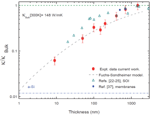
was monitored as a function of the absorbed power. For this purpose, the absorption coefficient of the membranes was experimentally determined and also theoretically modelled. A systematic decrease in the thermal conductivity was observed as reducing the thickness of the membranes which is explained using the Fuchs-Sondheimer model through the influence of phonon boundary scattering at the surfaces. The thermal conductivity of the thinnest membrane with d=9 nm resulted in 9±2 W/mK, thus approaching the amorphous limit but still maintaining a high crystalline quality.
APL Materials 2, 012113 (Jan. 31, 2014)
|
|
|
2013
(49) Effects of strain on the valence band structure and exciton-polariton energies in ZnO
M. R. Wagner1,2, G. Callsen1, J. S. Reparaz1,2, R. Kirste1,3, A. Hoffmann1, A. V. Rodina4, A. Schleife5,6,7, F. Bechstedt6,7, M. R. Phillips8
1 Institute of Solid State Physics, Technische Universität Berlin, Hardenbergstr. 36, 10623 Berlin, Germany
2 ICN2 - Institut Catala de Nanociencia i Nanotecnologia, Campus UAB, 08193 Bellaterra (Barcelona), Spain
3 Department of Material Science and Engineering, NCSU, 1001 Capability Dr., Raleigh, North Carolina 27695, USA
4 A. F. Ioffe Physico-Technical Institute, 194021 St. Petersburg, Russia
5 Condensed Matter and Materials Division, Lawrence Livermore National Laboratory, Livermore, CA 94550, USA
6 Institut für Festkörpertheorie und -optik, Friedrich-Schiller-Universität, 07743 Jena, Germany
7 European Theoretical Spectroscopy Facility (ETSF)
8 Department of Physics and Advanced Materials, University of Technology Sydney, P.O. Box 123, Broadway, NSW 2007, Australia
|
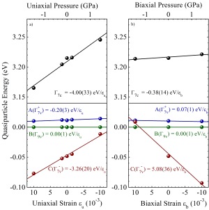
The uniaxial stress dependence of the band structure and the exciton-polariton transitions in wurtzite ZnO is thoroughly studied using modern first-principles calculations based on the HSE+G0W0 approach, k · p modeling using the deformation potential framework, and polarized photoluminescence measurements. The ordering of the valence bands (A(G7), B(G9), C(G7)) is found to be robust even for high uniaxial and biaxial strains. Theoretical results for the uniaxial pressure coefficients and splitting rates of the A, B, and C valence bands and their optical transitions are obtained including the effects of the spin-orbit interaction. The excitonic deformation potentials are derived and the stress rates for hydrostatic pressure are determined based on the results for uniaxial and biaxial stress. In addition, the theory for the stress dependence of the exchange interaction and longitudinal-transversal splitting of the exciton-polaritons is developed using the basic exciton functions of the quasi-cubic approximation and taking the interaction between all exciton states into account. It is shown that the consideration of these effects is crucial for an accurate description of the stress dependence of the optical spectra in ZnO. The theoretical results are compared to polarized photoluminescence measurements of different ZnO substrates as function of uniaxial pressure and experimental values reported in the literature demonstrating an excellent agreement with the computed pressure coefficients.
Physica Review B 88, 235210 (Dec. 30, 2013)
|
|
|
(48) Li-doped ZnO nanorods with single-crystal quality non-classical crystallization and self-assembly into mesoporous materials
C. Lizandara-Pueyo1, S. Dilger1, M. R. Wagner2,3, M. Gerigk1, A. Hoffmann2, and Sebastian Polarz2
1 University of Konstanz, Universitaetsstr. 10, 78464 Konstanz, German
2 Institut für Festkörperphysik, Technische Universität Berlin, Hardenbergstr. 36, 10623 Berlin, Germany
3 ICN2 - Institut Catala de Nanociencia i Nanotecnologia, Campus UAB, 08193 Bellaterra (Barcelona), Spain
|
The benefits and promise of nanoscale dimensions for the properties of (ceramic) semiconductors are widely known. 1-D nanostructures in particular have proven to be of extraordinary relevance due to their applicability in future electronic and optoelectronic devices. Key to successful technological implementation of semiconductor nanostructures is the control of their electronic properties via doping. Despite its tremendous importance, precise chemical doping of defined nano-objects has been addressed rarely so far. Frequent problems are the creation of secondary defects and related undesired property changes by incorporation of hetero-elements, and the difficulty in ensuring a uniform and precise positioning of the dopant in the nanocrystal lattice. Here, we present the synthesis of Li-doped zinc oxide nanorods, which possess excellent (single-crystal) quality. The method is based on a novel non-classical crystallization mechanism, comprising an unusually oriented disassembly step. Afterwards, the nanorods are incorporated into mesoporous layers using colloidal self-assembly. Proof-of-principle gas sensing measurements with these novel materials demonstrate the beneficial role of Li-doping, indicating not only better conductivity but also the occurrence of catalytic effects.
Crystal Engineering Communications 16, 1525 (Oct. 22, 2013)
|
|
|
(47) SrTiO3 thin films as highly efficient thermoelectric materials
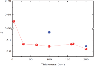
S. Bhansali1, W. Khunsin1, J. S. Reparaz1, M. R. Wagner1, J. Roqueta2, J. Santiso2, B. Abad Mayor3, P. Díaz-Chao3, M. Martin-Gonzalez3, and C. M. Sotomayor Torres1,4
1 ICN2 - Institut Catala de Nanociencia i Nanotecnologia, Campus UAB, 08193 Bellaterra (Barcelona), Spain
2 Centre dInvestigació en Nanociencia i nanotecnología (CIN2), Campus UAB, 08193 (Bellaterra) Barcelona, Spain
3 Thermoelectrics Research Group, Instituto de Microelectronica de Madrid, CSIC, Madrid, Spain
4 Institució Catalana de Recerca i Estudis Avançats (ICREA), 08010 Barcelona, Spain
|
In his work we investigate the thermoelectric performance of SrTiO3 thin films doped with Nb grown using pulsed laser deposition on crystalline LaAlO3 substrates. We show that a large enhancement of the Seebeck coefficient is observed for thin films with thicknesses below 10 nm in accordance with previous publications. In addition, we investigated the thermal conductivity of the thin films using the 3omega technique between 4 and 300 K. We show that the thermal conductivity is reduced by a factor of three with respect to the bulk value. This reduction originates mostly in structural defects and oxygen vacancies
within the thin films. Finally, the figure of merit of the thinnest films at 300 K resulted in ZT=0.62.
IEEE Therminic 19, 359 (Sept. 25, 2013)
|
|
|
(46) Thermal conductivity reduction in Si free-standing membranes investigated using Raman thermometry
J. S. Reparaz1, E. Chavez-Angel1,2, J. Gomis-Bresco1, M. R. Wagner1, A. Shchepetov3, M. Prunnila3, J. Ahopelto3, F. Alzina1, and C. M. Sotomayor-Torres1,4
1 ICN2 - Institut Catala de Nanociencia i Nanotecnologia, Campus UAB, 08193 Bellaterra (Barcelona), Spain
2 Dept. of Physics, UAB, 08193 Bellaterra (Barcelona), Spain
3 VTT Technical Research Centre of Finland, PO Box 1000, 02044 VTT, Espoo, Finland
4 Institució Catalana de Recerca i Estudis Avançats (ICREA), 08010 Barcelona, Spain
|
We report on the reduction of the thermal conductivity in ultra-thin suspended Si membranes with high crystalline quality at room temperature. A series of membranes with thicknesses ranging from 9 nm to 1.5 ?m was investigated using Raman thermometry, a novel contactless optical technique for thermal conductivity determination. The temperature rise of a laser spot focused on the membranes was monitored as a function of the absorbed power. For this purpose, the absorption coefficient of the membranes was experimentally determined and also theoretically modelled. A systematic decrease in the thermal conductivity was observed as reducing the thickness of the membranes which is explained using the Fuchs-Sondheimer model through the influence of phonon boundary scattering at the surfaces of the membranes. The thermal conductivity of the thinnest membrane with d= 9 nm resulted in (9±2)W/mK, thus approaching the amorphous limit but still maintaining a high crystalline quality.
IEEE Therminic 19, 95 (Sept. 25, 2013)
|
|
|
(45) Nanoscale thermal transport and phonon dynamics in ultra-thin Si based nanostructures
M. R. Wagner1, E. Chavez-Angel1,2, J. Gomis-Bresco1, J. S. Reparaz1, A. Shchepetov3, M. Prunnila3, J. Ahopelto3, F. Alzina1, and C. M. Sotomayor-Torres1,4
1 ICN2 - Institut Catala de Nanociencia i Nanotecnologia, Campus UAB, 08193 Bellaterra (Barcelona), Spain
2 Dept. of Physics, UAB, 08193 Bellaterra (Barcelona), Spain
3 VTT Technical Research Centre of Finland, PO Box 1000, 02044 VTT, Espoo, Finland
4 Institució Catalana de Recerca i Estudis Avançats (ICREA), 08010 Barcelona, Spain
|
We study the dynamics of acoustic phonons in ultra-thin free-standing silicon membranes both experimentally and theoretically. We discuss the impact of the lifetimes of the acoustic phonons on the thermal transport properties of the membranes with thicknesses ranging from 8 nm to 1.5 ?m. The phonon lifetimes are determined by measuring the dynamic variation of the reflectivity using ultra-fast pump-probe spectroscopy. This is achieved by asynchronous optical sampling (ASOPS) of two actively coupled femto-second laser oscillators. The coherent acoustic phonon lifetime is obtained from the dynamical variations of the reflectivity with a sensitivity of 10-5 and a time resolution of about 50 fs. The experimental results are compared to theoretical calculations considering both intrinsic and extrinsic relaxation scattering processes.
IEEE Therminic 19, 10 (Sept. 25, 2013)
|
|
|
(44) Nitrogen and vacancy clusters in ZnO (Invited Feature Paper)
F. Tuomisto1, C. Rauch1, M. R. Wagner2,3, A. Hoffmann3, S. Eisermann4, B. K. Meyer4, L. Kilanski5, M. C. Tarun6, and M. D. McCluskey6
1 Department of Applied Physics, Aalto University, P.O. Box 11100, FI-00076 Aalto, Finland
2 ICN2 - Institut Catala de Nanociencia i Nanotecnologia, Campus UAB, 08193 Bellaterra (Barcelona), Spain
3 Institut für Festkörperphysik, Technische Universität Berlin, Hardenbergstr. 36, 10623 Berlin, Germany
4 I. Physics Institute, Justus-Liebig-University Giessen, Heinrich Buff Ring 16, 35392 Giessen, Germany
5 Institute of Physics, Polish Academy of Sciences, Al. Lotnikow 32/46, 02-668 Warsaw, Poland
6 Department of Physics and Astronomy, Washington State University, Pullman, WA 99164-2814, USA
|
Understanding the interaction of group V impurities with intrinsic defects in ZnO is important for developing p-type material. We have studied N-doped ZnO thin films and N-doped bulk ZnO crystals, with positron annihilation spectroscopy, in contrast to earlier studies that have concentrated on N-implanted ZnO crystals. We show that the introduction of N impurities into ZnO, irrespective of whether it is done during the growth of thin films or bulk crystals or through implantation and subsequent thermal treatments, leads to the formation of stable vacancy clusters and negative ion-type defects. Interestingly, the stability of these vacancy clusters is found almost exclusively for N introduction, whereas single Zn vacancy defects or easily removable vacancy clusters are more typically found for ZnO doped with other impurities.
Journal of Materials Research 28, 1977 (Jul. 23, 2013)
|
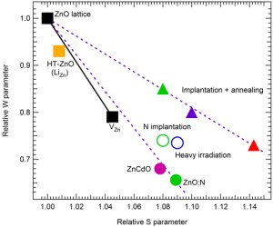
|
|
(43) Steering photon statistics in single quantum dots: From one- to two-photon emission (Editor's Choice)
G. Callsen1, A. Carmele1, G. Honig1, J. Brunnmeier1, C. Kindel1, M. R. Wagner1, E. Stock1, J. S. Reparaz1, A. Schliwa1, S. Reitzenstein1, A. Knorr1, A. Hoffmann1, S. Kako2, and Y. Arakawa2
1 Institut für Festkörperphysik, Technische Universität Berlin, Hardenbergstr. 36, 10623 Berlin, Germany
2 Institute of Industrial Science, University of Tokyo, 4-6-1 Komaba, Meguro-ku, Tokyo 153-8505, Japan
|
We present a combined experimental and theoretical study of two-photon emission from the biexciton cascade in single GaN quantum dots. By changing the biexciton binding energy, pump power and temperature, the balance between the one- and two-photon decay processes is controlled in this 4-level system, which drastically affects the photon statistics of the resulting emission. As most pronounced feature of this interplay we observe a bunching phenomenon and a transition from sub- to super-Poissonian photon statistics, originating from the complex nature of the biexciton cascade. This work highlights how photon-statistics can be steered between one- and two-photon processes towards an increased, bunched two-photon emission probability up to 50 K with the perspective of photon pair generation in the UV spectral range.
Physical Review B 87, 245314 (Jun. 26, 2013)
|
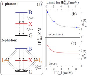
|
|
(42) Nanoscale imaging of InN segregation and polymorphism in single vertically aligned InGaN/GaN multi quantum well
nanorods by tip-enhanced Raman scattering
E. Poliani1, M. R. Wagner1,2, J. S. Reparaz1,2, M. Mandl3, M. Strassburg3, X. Kong4, A. Trampert4, C. M. Sotomayor Torres2,5, A. Hoffmann1, and J. Maultzsch1
1 Institut für Festkörperphysik, Technische Universität Berlin, Hardenbergstr. 36, 10623 Berlin, Germany
2 ICN2 - Institut Catala de Nanociencia i Nanotecnologia, Campus UAB, 08193 Bellaterra (Barcelona), Spain
3 OSRAM Opto Semiconductors GmbH, 93055 Regensburg, Germany
4 Paul Drude Insitute, 10117 Berlin, Germany
6 Institució Catalana de Recerca I Estudis Avançats (ICREA), 08010 Barcelona, Spain
|
Vertically aligned GaN nanorod arrays with nonpolar InGaN/GaN multi quantum wells (MQW) were grown by MOVPE on c-plane GaN-on-sapphire templates. The chemical and structural properties of single nanorods are optically investigated with a spatial resolution beyond the diffraction limit using tip-enhanced Raman spectroscopy (TERS). This enables the local mapping of variations in the chemical composition, charge distribution, and strain in the MQW region of the nanorods. Nanoscale fluctuations of the In content in the InGaN layer of few percents can be identified and visualized with a lateral resolution below 35 nm. We obtain evidence for the presence of indium clustering and the formation of cubic inclusions in the wurtzite matrix near the QW layers. These results are directly confirmed by high-resolution TEM images, revealing the presence of stacking faults and different polymorphs close to the surface near the MQW region. The combination of TERS and HRTEM demonstrates the potential of this nanoscale near-field imaging technique, establishing TERS as very potent, comprehensive, and non-destructive tool for the characterization and optimization of technologically relevant semiconductor nanostructures.
Nano Letters 13, 3205 (Jun. 24, 2013)
|
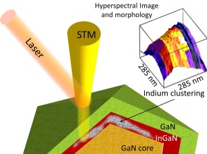
|
|
(41) Spatial mapping of exciton lifetimes in single ZnO nanowires (Research Highlight)
J. S. Reparaz1,2, G. Callsen1, M. R. Wagner1,2 F. Güell4, J. R. Morante4,5 C. M. Sotomayor Torres2,3 and A. Hoffmann1
1 Institut für Festkörperphysik, Technische Universität Berlin, Hardenbergstr. 36, 10623 Berlin, Germany
2 ICN2 - Institut Catala de Nanociencia i Nanotecnologia, Campus UAB, 08193 Bellaterra (Barcelona), Spain
3 ICREA, Passeig Lluis Companys 23, 08010 Barcelona, Spain
4 Departament dElectronica, M-2E, IN2UB, Universitat de Barcelona, C/Marti Franques 1, 08028 Barcelona, Spain
5 Institut de Recerca en Energia de Catalunya (IREC), Jardins de les Dones de Negre 1, 08930 Sant Adria de Besos, Spain
|
We investigate the spatial dependence of the exciton lifetimes in single ZnO nanowires. We have found that the free exciton and bound exciton lifetimes exhibit a maximum at the center of nanowires while they decrease by 30\% towards the tips. This dependence is explained by considering the cavity-like properties of the nanowires in combination with the Purcell effect. We show that the lifetime of the bound-excitons scales with the localization energy to the power of 3/2 which validates the model of Rashba and Gurgenishvili at the nanoscale.
APL Materials 1, 012103 (Jun. 06, 2013)
|
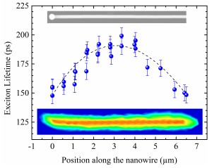
|
|
(40) Structural and optical investigation of non-polar (1-100) GaN grown by the ammonothermal method
D. Gogova1, P. P. Petrov1, M. Buegler2, M. R. Wagner2,3, C. Nenstiel2,4, G. Callsen2, M. Schmidbauer1, R. Kucharski5, M. Zajac5, R. Dwilinski5, M. R. Phillips4, A. Hoffmann2 and R. Fornari1
1 Leibniz Institute for Crystal Growth, Max-Born-Str. 2, 12489 Berlin, Germany
2 Institut für Festkörperphysik, Technische Universität Berlin, Hardenbergstr. 36, 10623 Berlin, Germany
3 ICN2 - Institut Catala de Nanociencia i Nanotecnologia, Campus UAB, 08193 Bellaterra (Barcelona), Spain
4 Department of Physics and Advanced Materials, University of Technology Sydney, P.O. Box 123, Broadway, NSW 2007, Australia
5 Ammono S.A., 2/31 Czerwonego Krzyza Str., 00-377 Warsaw, Poland
|
We studied the structural and optical properties of state-of-the-art non-polar bulk GaN grown by the ammonothermal method. The investigated samples have an extremely low dislocation density (DD) of less than 5 x 104 cm-2, which results in very narrow high-resolution x-ray rocking curves. The a and c lattice parameters of these stress-free GaN samples were precisely determined by using an x-ray diffraction technique based on the modified Bond method. The obtained values are compared to the lattice parameters of free-standing GaN from different methods and sources. The observed differences are discussed in terms of free-electron concentrations, point defects, and DD. Micro Raman spectroscopy revealed a very narrow phonon linewidth and negligible built-in strain in accordance with the high-resolution x-ray diffraction data. The optical transitions were investigated by cathodoluminescence measurements. The analysis of the experimental data clearly demonstrates the excellent crystalline perfection of ammonothermal GaN material and its potential for fabrication of non-polar substrates for homoepitaxial growth of GaN based device structures.
Journal of Applied Physics 113, 203513 (May 29, 2013)
|
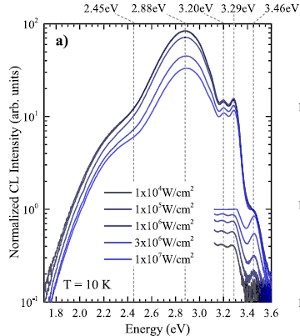
|
|
(39) Probing local strain and composition in Ge nanowires by means of tip-enhanced Raman scattering
J. S. Reparaz1,2, N. Peica1, R. Kirste1, A. R. Goni2,3, M. R. Wagner1, G. Callsen1, M. I. Alonso1,2, M. Garriga2, I. C. Marcus2, A. Ronda4, I. Berbezier4, J. Maultzsch1, C. Thomsen1, and A. Hoffmann1
1 Institut für Festkörperphysik, Technische Universität Berlin, Hardenbergstr. 36, 10623 Berlin, Germany
2 Institut de Ciencia de Materials de Barcelona, ICMAB-CSIC, Esfera UAB, 08193 Bellaterra, Spain
3 ICREA, Passeig Lluis Companys 23, 08010 Barcelona, Spain
4 IM2NP, CNRS - Univ. Aix Marseille, Campus St. Jerome, Case 142, 13397 Marseille Cedex 20, France
|
Local strain and Ge content distribution in self-assembled, in-plane Ge/Si nanowires (NWs) grown by combining molecular beam epitaxy and the metal-catalyst assisted-growth method were investigated by tip-enhanced Raman scattering (TERS). We show that this technique is essential to study variations of physical properties of single wires at the nanoscale, a task which cannot be achieved with conventional micro-Raman scattering. As two major findings we report that: i) The Ge distribution in the (001) crystallographic direction is inhomogeneous, displaying a gradient with a higher Ge content close to the top surface. ii) In contrast, the (uncapped) wires exhibit essentially the same small residual compressive strain everywhere along the wire.
Nanotechnology 24, 185704 (Apr. 11, 2013)
|
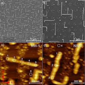
|
|
(38) Compensation effects in GaN:Mg probed by Raman spectroscopy and photoluminescence measurements
R. Kirste1,2, M. P. Hoffmann2, J. Tweedie2, Z. Bryan2, G. Callsen1, T. Kure1, C. Nenstiel1, M. R. Wagner1, R. Collazo2, A. Hoffmann1, and Zlatko Sitar2
1 Institut für Festkörperphysik, Technische Universität Berlin, Hardenbergstr. 36, 10623 Berlin, Germany
2 Department of Material Science and Engineering, NCSU, 1001 Capability Dr., Raleigh, North Carolina 27695, USA
|
Compensation effects in metal organic chemical vapour deposition grown GaN doped with magnesium are investigated with Raman spectroscopy and photoluminescence measurements. Examining the strain sensitive E2(high) mode, an increasing compressive strain is revealed for samples with Mg-concentrations lower than 7x1018cm-3. For higher Mg-concentrations, this strain is monotonically reduced. This relaxation is accompanied by a sudden decrease in crystal quality. Luminescence measurements reveal a well defined near band edge luminescence with free, donor bound, and acceptor bound excitons as well as a characteristic donor acceptor pair (DAP) luminescence. Following recent results, three acceptor bound excitons and donor acceptor pairs are identified. Along with the change of the strain, a strong modification in the luminescence of the dominating acceptor bound exciton and DAP luminescence is observed. The results from Raman spectroscopy and luminescence measurements are interpreted as fingerprints of compensation effects in GaN:Mg leading to the conclusion that compensation due to defect incorporation triggered by Mg-doping already affects the crystal properties at doping levels of around 7x1018cm-3. Thereby, the generation of nitrogen vacancies is introduced as the driving force for the change of the strain state and the near band edge luminescence.
Journal of Applied Physics 113, 103504 (Mar. 08, 2013)
|
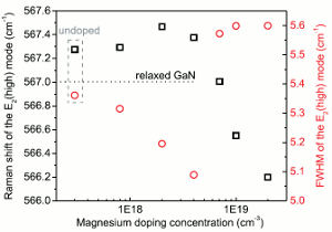
|
|
2012
(37) Effect of TMGa preflow on the properties of high temperature AlN layers grown on sapphire
R. Kirste1, M. R. Wagner1, C. Nenstiel1, F. Brunner2, M. Weyers2, A. Hoffmann1
1 Institut für Festkörperphysik, Technische Universität Berlin, Hardenbergstr. 36, 10623 Berlin, Germany
2 Ferdinand Braun Institut, Gustav-Kirchhoff Str. 4, 12489 Berlin, Germany
|
The effect of a trimethylgallium (TMGa) preflow on the structural and optical properties of MOCVD grown AlN layers on sapphire substrates is investigated. Secondary ion mass spectroscopy measurements were performed to investigate the incorporation of Ga in the layers. It is shown that for AlN layers grown with a TMGa preflow Ga atoms incorporate mainly near the substrate/epilayer interface. Photoluminescence spectra exhibit a free exciton and a donor bound exciton. By analyzing the full width at half maximum of the free exciton and the defect luminescence an increased optical quality for the sample grown with TMGa preflow is demonstrated. Additionally, Raman spectroscopy reveals a higher crystal quality for this sample. Comparing the results from Raman spectroscopy and luminescence measurements a shift rate of 60meV/GPa-1 is determined for the free A-exciton. Finally, cross-sectional Raman spectroscopy is used to compare the strain at the AlN/sapphire interface for a sample grown with and without TMGa preflow.
Physica Status Solidi A 210, 285 (Oct. 25, 2012)
|
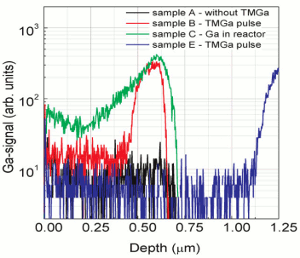
|
|
(36) Optical signature of Mg-doped GaN: Transfer processes
G. Callsen1, M. R. Wagner1, T. Kure1, J. S. Reparaz1, M. Buegler1, J. Brunnmeier1, C. Nenstiel1, A. Hoffmann1, M. Hoffmann2, J. Tweedie2, Z. Bryan2, S. Aygun2, R. Kirste2, R. Collazo2, and Z. Sitar2
1 Institut für Festkörperphysik, Technische Universität Berlin, Hardenbergstr. 36, 10623 Berlin, Germany
2 Material Science and Engineering, North Carolina State University, Raleigh, North Carolina, United States
|
Mg doping of high quality, metal organic chemical vapor deposition grown GaN films results in distinct traces in their photoluminescence and photoluminescence excitation spectra. We analyze GaN:Mg grown on sapphire substrates and identify two Mg related acceptor states, one additional acceptor state and three donor states that are involved in the donor-acceptor pair band transitions situated at 3.263.29 eV in GaN:Mg. The presented determination of the donor-acceptor pair band excitation channels by photoluminescence excitation spectroscopy in conjunction with temperature-dependent photoluminescence measurements results in a direct determination of the donor and acceptor binding, localization, and activation energies, which is put into a broader context based on Haynes's rule. Furthermore, we analyze the biexponential decay dynamics of the photoluminescence signal of the acceptor and donor bound excitons. As all observed lifetimes scale with the localization energy of the donor and acceptor related bound excitons, defect and complex bound excitons can be excluded as their origin. Detailed analysis of the exciton transfer processes in the close energetic vicinity of the GaN band edge reveals excitation via free and bound excitonic channels but also via an excited state as resolved for the deepest localized Mg related acceptor bound exciton. For the two Mg acceptor states, we determine binding energies of 164 ± 5 and 195 ± 5 meV, which is in good agreement with recent density functional theory results. This observation confirms and quantifies the general dual nature of acceptor states in GaN based on the presented analysis of the photoluminescence and photoluminescence excitation spectra.
Physical Review B 86, 235204 (Aug. 23, 2012)
|
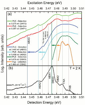
|
|
(35) Phonon plasmon interaction in ternary group-III-nitrides
R. Kirste1, S. Mohn1, M. R. Wagner1, J. S. Reparaz1, and A. Hoffmann1
1 Institut für Festkörperphysik, Technische Universität Berlin, Hardenbergstr. 36, 10623 Berlin, Germany
|
Phonon-plasmon-coupling in the ternary group-III-nitrides InGaN and AlGaN is investigated experimentally and theoretically. Based on the observation of broadening and shifting of the A1(LO) mode in AlGaN upon Si-doping, a lineshape analysis was performed to determine the carrier concentration. The results obtained by this method are in excellent agreement to those from Hall measurements, confirming the validity of the employed model. Finally, neglecting phonon and plasmon damping, the Raman shift of the A1(LO) mode in dependence of the carrier concentration for AlGaN
and InGaN is calculated. This enables a fast and contactless determination of carrier concentrations in the future.
Applied Physics Letters 101, 041909 (Jul. 26, 2012)
|
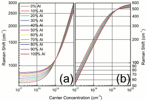
|
|
(34) Optical signatures of nitrogen acceptors in ZnO
S. Lautenschlaeger1, S. Eisermann1, G. Haas1, E. A. Zolnowski1, M. N. Hofmann1, A. Laufer1, M. Pinnisch1, B. K. Meyer1, M. R. Wagner2, J. S. Reparaz2, G. Callsen2, A. Hoffmann2, A. Chernikov3, S. Chatterjee3, V. Bornwasser3, and M. Koch3
1 I. Physikalisches Institut, Justus-Liebig-Universität Gießen, Heinrich-Buff-Ring 16, 35392 Gießen, Germany
2 Institut für Festkörperphysik, Technische Universität Berlin, Hardenbergstr. 36, 10623 Berlin, Germany
3 Faculty of Physics and Materials Sciences Center, Philipps University Marburg, Renthof 5, 35032 Marburg, Germany
|
We report on the optical properties of nitrogen acceptor-doped ZnO epilayers in the medium and high doping regimes using temperature and excitation power-dependent, as well as time-resolved photoluminescence experiments. The epilayers were doped with ammonia during homoepitaxial growth on ZnO single-crystal substrates with different surface polarities. Significant differences in the optical characteristics of the epilayers are observed between growth on nonpolar a-plane, polar c-plane Zn-face substrates and polar c-plane O-face substrates, which demonstrates different incorporation of the nitrogen acceptor depending on the substrate polarity. The incorporation of nitrogen into the ZnO films ranges between 1019 and 1021 cm-3 as determined by secondary ionmass spectrometry.Within this doping range the samples change from lightly compensated to highly doped compensated.We discuss the unique photoluminescence features of nitrogen-doped ZnO epilayers within the concept of shallow donor-acceptor-pair recombinations and at the highest doping level by the appearance of potential fluctuations.
Physical Review B 85, 235204 (Jun. 21, 2012)
|
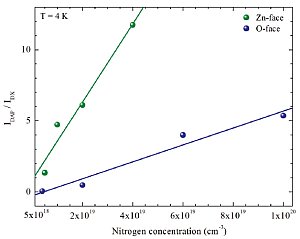
|
|
(33) Band-gap engineering of zinc oxide colloids via lattice substitution with sulfur leading to materials with advanced properties for optical applications like full inorganic UV protection
D. Lehr1, M. Luka1, M. R. Wagner2, M. Buegler2, A. Hoffmann2, and S. Polarz1
1 University of Konstanz, Universitaetsstr. 10, 78464 Konstanz, German
2 Institut für Festkörperphysik, Technische Universität Berlin, Hardenbergstr. 36, 10623 Berlin, Germany
|
The advanced application of wide-band gap semiconductors in areas like photovoltaics, optoelectronics, or photocatalysis requires a precise control over electronic properties. Zinc oxide is favorable for large-scale technological applications now and in the future because of the large, natural abundance of the involved, chemical elements. Often it is important that the band gap can be controlled precisely. While a blue-shift of the band gap can be reached quite easily using the quantum-size effect, it is still very difficult to achieve a redshift. We present a powerful method for the band gap engineering of ZnO via the incorporation of sulfur as a solid solutions. The reduction of the energy gap is controlled by ZnO1-xSx composition, whereas the latter is adjusted via special organometallic precursor molecules. The material can be supplied in a continuous fashion and in a more refined morphology, for instance spherical ZnO1-xSx colloids with sizes below lambdavis/2 (about 200 nm). As a concrete application of contemporary importance first steps toward the full inorganic UV protection are made.
Chemistry of Materials 24, 1771 (May 02, 2012)
|
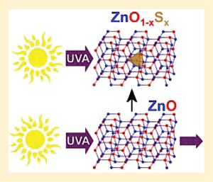
|
|
2011
(32) Temperature dependent photoluminescence of lateral polarity junctions of MOVPE grown GaN
R. Kirste1, R. Collazo2, G. Callsen1, M. R. Wagner1, T. Kure1, J. S. Reparaz1, S. Mita3, J. Xie3, A. Rice2, J. Tweedie2, Z. Sitar2, A.Hoffmann1
1 Institut für Festkörperphysik, Technische Universität Berlin, Hardenbergstr. 36, 10623 Berlin, Germany
2 Department of Materials Science and Engineering, North Carolina State University, Raleigh, NC 27695, USA
3 HexaTech, Inc., 991 Aviation Pkwy., Suite 800, Morrisville, NC 27560, USA
|
We report on fundamental structural and optical properties of lateral polarity junctions in GaN. GaN with Ga- to N-polar junctions was grown on sapphire using an AlN buffer layer. Results from scanning electron microscopy and Raman spectroscopy measurements indicate a superior quality of the Ga-polar GaN. An extremely strong luminescence signal is observed at the inversion domain boundary (IDB). Temperature dependent micro photoluminescence measurements are used to reveal the recombination processes underlying this strong emission. At 5 K the emission mainly arises from a stripe along the inversion domain boundary with a thickness of 4-5 ìm. An increase of the temperature initially leads to a narrowing to below 2 µm emission area width followed by a broadening at temperatures above 70 K. The relatively broad emission area at low temperatures is explained by a diagonal IDB. It is shown that all further changes in the emission area width are related to thermalization effects of carriers and defects attracted to the IDB. The results are successfully used to confirm a theoretical model for GaN based lateral polarity junctions. Due to the strong and pronounced emission of IDBs even at elevated temperatures it is demonstrated that lateral polarity junctions exhibit a strong potential for future high efficiency devices.
Journal of Applied Physics 110, 093503 (Nov. 02, 2011)
|
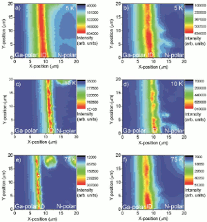
|
|
(31) Decay dynamics of excitonic polarons in InAs/GaAs Quantum Dots
S. Werner1, J. S. Reparaz1, M. R. Wagner1, P. Zimmer1, N. N. Ledentsov1, J. Kabuss2, M. R. Dachner2, M. Richter2, A. Knorr2, C. Thomsen1, A. Hoffmann1
1 Institut für Festkörperphysik, Technische Universität Berlin, Hardenbergstr. 36, 10623 Berlin, Germany
2 Institut für Theoretische Physik, Technische Universität Berlin, Hardenbergstr. 36, 10623 Berlin, Germany
|
We present time-resolved studies of the exciton-phonon interaction in self-assembled InAs/GaAs quantum dots. Different scattering and luminescence processes were investigated by time-resolved spectroscopy exciting resonantly into the quantum dots electronic structure. Studying the characteristic decay times of the ground state and of several phonon-assisted recombinations we were able to distinguish a resonant Raman process from a phonon-assisted photoluminescence process which are always simultaneously present and can interfere with each other. While lifetimes under 30 ps were observed for the coherent Raman process, the incoherent phonon-assisted recombination exhibited typical lifetimes of around 1 ns independently of the excitation energy. We conclude that under resonant excitation the dominant radiative recombination process in this system always involves an electronic state of the ground state of the quantum dots electronic structure. Combiningtemperature-dependent and time-resolved measurements we show that a weak phonon-bottleneck is present in the low temperature regime (<130 K), while it disappears for higher temperatures.
Journal of Applied Physics 110, 074303 (Oct. 03, 2011)
|
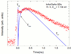
|
|
(30) Titanium assisted growth of silica nanowires: from surface-matched to free-standing morphologies
G. Callsen1, J. S. Reparaz1, M. R. Wagner1,2, A. Vierck1, M. R. Phillips2, C. Thomsen1 and A. Hoffmann1
1 Institut für Festkörperphysik, Technische Universität Berlin, Hardenbergstr. 36, 10623 Berlin, Germany
2 Department of Physics and Advanced Materials, University of Technology Sydney, P.O. Box 123, Broadway, NSW 2007, Australia
|
We report on an oxide-assisted growth technique for silica nanowires which allows tuning the growth from lattice-matched nanowires to free-standing morphologies based on growth control by Ti in the role of a catalyst and surfactant. Due to an adjustable Ti concentration we grew silica nanowires with lengths ranging from 100 nm up to several millimetres whose defect chemistry was analyzed by electron microscopy tools, monochromatic cathodoluminescence imaging and time resolved photoluminescence spectroscopy. The knowledge of the luminescence properties and the related defect occurrence along with their spatial distribution is pivotal for advancing silica nanowire growth in order to realize successful device designs based on self-assembled Si/SiOx nanostructures. We demonstrate a core-shell structure of the grown nanowires with a highly luminescent 150 nm thick shell and outstandingly fast decaying dynamics (.1 ns) for glass-like materials. The conjunction of the observed efficient and stable luminescences with their attributed decaying behaviours suggests applications for silica nanowires like active and passive optical interconnectors and white light phosphors. The identification of a time domain difference for the spectral regime from 2.3 to 3.3 eV, within the confined spatial dimensions of a single nanowire, is very promising for future device applications employing silica nanowires which exhibit unique compatibility with commonly applied silicon based electronics. A qualitative growth model based on silica nanoparticle diffusion and Ti assisted seed formation is developed for the various types of segregated silica nanowires which extends commonly assumed oxide-assisted growth mechanisms.
Nanotechnology 22, 405604 (Sept. 13, 2011)
|
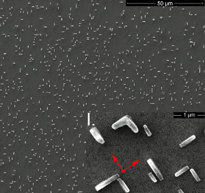
|
|
(29) Assembly of carbon nanotubes and alkylated-fullerenes: Nanocarbon-hybrid towards photovoltaic applications
Y. Shen1, J. S. Reparaz2, M. R. Wagner2, A. Hoffmann2, C. Thomsen2, J. O. Lee3, S. Heeg4, B. Hatting4, S. Reich4, A. Saeki5, S. Seki5, K. Yoshida6, S. S. Babu1, H. Möhwald7, T. Nakanishi1
1 National Institute for Materials Science (NIMS), 1-2-1 Sengen, Tsukuba, 305-0047, Japan
2 Technische Universität Berlin, Hardenbergstr. 36, 10623 Berlin, Germany
3 Korea Research Institute of Chemical Technology, Daejeon, 305-343, Korea
4 Freie Universität Berlin, 14195 Berlin, Germany
5 Graduate School of Engineering, Osaka University, Osaka, Japan
6 Institute for Chemical Science, Kyoto University, Kyoto, Japan
7 Max Planck Institute of Colloids and Interfaces, 14424 Potsdam, Germany
|
Taking advantage of the noncovalent interaction between alkyl chain and sidewall of single-walled carbon nanotubes (SWCNT), a nanocarbon hybrid of SWCNT and a fullerene (C60) derivative with long alkyl chains was constructed as a donor-acceptor pair for photovoltaics and nanodevice investigations. It was found that SWCNT could be mostly unbundled by the alkylated C60 (1) and well-dispersed in organic solvents. As photoactive materials, the resultant nanocarbon hybrid, 1-SWCNT, performed well for light-energy harvesting applications in photoelectrochemical cells and nanoscaled field-effect transistors (FET). Moreover, the 1-SWCNT assembly exhibited superhydrophobicity, providing the interesting opportunity to fabricate nanocarbon-based water-proof optoelectronic devices. In order to understand the photoexcitation process, the 1-SWCNT assembly was characterized electrochemically and spectroscopically. Electrochemical results showed that the SWCNT facilitated electronic communication between 1 and electrode. The steady-state and time-resolved fluorescence, and the photoluminescence excitation studies suggested efficient quenching of the singlet excited state of C60. Nanosecond transient absorption data revealed the one-electron reduction of fullerene, C60-, thereby demonstrating the photoinduced electron transfer from SWCNT to the C60 unit in the 1-SWCNT assembly.
Chemical Science 02, 2243 (Aug. 25, 2011)
|
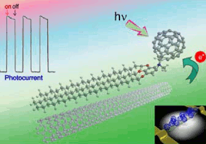
|
|
(28) Bound excitons in ZnO: Structural defect complexes versus shallow impurity centers
M. R. Wagner1,3, G. Callsen1, J. S. Reparaz1, J.-H. Schulze1, R. Kirste1, M. Cobet1, I. A. Ostapenko1, S. Rodt1, C. Nenstiel1,3, M. Kaiser1, A. Hoffmann 1, A. V. Rodina2, M. R. Phillips3, S. Lautenschläger4, S. Eisermann4, B. K. Meyer4
1 Institute of Solid State Physics, Technische Universität Berlin, Hardenbergstr. 36, 10623 Berlin, Germany
2 A. F. Ioffe Physico-Technical Institute, 194021 St. Petersburg, Russia
3 Department of Physics and Advanced Materials, University of Technology Sydney, P.O. Box 123, Broadway, NSW 2007, Australia
4 I. Physikalisches Institut, Justus-Liebig-Universität Gießen, Heinrich-Buff-Ring 16, 35392 Gießen, Germany
|
ZnO single crystals, epilayers, and nanostructures often exhibit a variety of narrow emission lines in the spectral range between 3.33 and 3.35 eV which are commonly attributed to deeply bound excitons (Y lines). In this work, we present a comprehensive study of the properties of the deeply bound excitons with particular focus on the Y0 transition at 3.333 eV. The electronic and optical properties of these centers are compared to those of the shallow impurity related exciton binding centers (I lines). In contrast to the shallow donors in ZnO, the deeply bound exciton complexes exhibit a large discrepancy between the thermal activation energy and localization energy of the excitons and cannot be described by an effective mass approach. The different properties between the shallow and deeply bound excitons are also reflected by an exceptionally small coupling of the deep centers to the lattice phonons and a small splitting between their two electron satellite transitions. Based on a multitude of different experimental results including magnetophotoluminescence, magnetoabsorption, excitation spectroscopy (PLE), time resolved photoluminescence (TRPL), and uniaxial pressure measurements, a qualitative defect model is developed which explains all Y lines as radiative recombinations of excitons bound to extended structural defect complexes. These defect complexes introduce additional donor states in ZnO. Furthermore, the spatially localized character of the defect centers is visualized in contrast to the homogeneous distribution of shallow impurity centers by monochromatic cathodoluminescence imaging. A possible relation between the defect bound excitons and the green luminescence band in ZnO is discussed. The optical properties of the defect transitions are compared to similar luminescence lines related to defect and dislocation bound excitons in other IIVI and IIIV semiconductors.
Physical Review B 84, 035313 (Jul. 26, 2011)
|
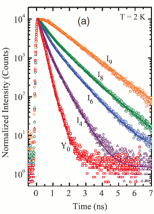
|
|
(27) Raman and photoluminescence spectroscopic detection of surface-bound Li+O2- defect sites in Li-doped ZnO nanocrystals derived from molecular precursors
R. Kirste1, Y. Aksu2, M. R. Wagner1, S. Khachadorian1, S. Jana2, M. Driess2, C. Thomsen1, A. Hoffmann1
1 Institute of Solid State Physics, Technische Universität Berlin, Hardenbergstr. 36, 10623 Berlin, Germany
2 Institute of Chemistry, TU Berlin, Straße des 17. Juni 135, 10623 Berlin, Germany
|
We present a detailed study of Raman spectroscopy and photoluminescence measurements on Li-doped ZnO nanocrystals with varying lithium concentrations. The samples were prepared starting from molecular precursors at low temperature. The Raman spectra revealed several sharp lines in the range of 100200 cm-1, which are attributed to acoustical phonons. In the high-energy range two peaks were observed at 735 cm-1 and 1090 cm-1. Excitation-dependent Raman spectroscopy of the 1090 cm-1 mode revealed resonance enhancement at excitation energies around 2.2 eV. This energy coincides with an emission band in the photoluminescence spectra. The emission is attributed to the deep lithium acceptor and intrinsic point defects such as oxygen vacancies. Based on the combined Raman and PL results, we introduce a model of surface-bound LiO2 defect sites, that is, the presence of Li+O2- superoxide. Accordingly, the observed Raman peaks at 735 cm-1 and 1090 cm-1 are assigned to Li-O and O-O vibrations of LiO2.
Chem. Phys. Chem. 12, 1189 (Mar. 23, 2011)
|
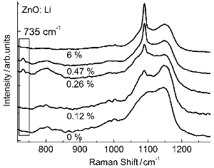
|
|
(26) Phonon deformation potentials in wurtzite GaN and ZnO determined by uniaxial pressure dependent Raman measurements
G. Callsen1, J. S. Reparaz1, M. R. Wagner1, R. Kirste1, C. Nenstiel1,2, A. Hoffmann1, M. R. Phillips2
1 Institute of Solid State Physics, Technische Universität Berlin, Hardenbergstr. 36, 10623 Berlin, Germany
1 Department of Physics and Advanced Materials, University of Technology Sydney, P.O. Box 123, Broadway, NSW 2007, Australia
|
We report the phonon deformation potentials of wurtzite GaN and ZnO for all zone center optical phonon modes determined by Raman measurements as a function of uniaxial pressure. Despite all the structural and optical similarities between these two material systems, the pressure dependency of their vibrational spectra exhibits fundamental distinctions, which is attributed to their different bond ionicities. In addition, the LO-TO splitting of the A1 and E1 phonon modes is analyzed which yields insight into the uniaxial pressure dependency of Borns transverse effective charge eT*.
Applied Physics Letters 98, 061906 (Feb. 09, 2011)
|
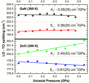
|
|
2010
(25) Shape anisotropy influencing functional properties: Trigonal prismatic ZnO nanoparticles as an example
C. Lizandara-Pueyo1, S. Siroky1, M. R. Wagner2, A. Hoffmann2, J. S. Reparaz2, M. Lehmann2, S. Polarz1
1 University of Konstanz, Universitaetsstr. 10, 78464 Konstanz, German
2 Institute of Solid State Physics, Technische Universität Berlin, Hardenbergstr. 36, 10623 Berlin, Germany
|
The shape of crystalline particles is recognized as one important parameter for the adjustment of functional properties of inorganic materials. The surfaces of a thermodynamically stable crystal correspond to a set of lattice planes determined by the minimum interface energy. Thus, a morphology deviating from the most stable state correlates to either a change of the proportion of those surfaces to each other or ultimately a new set of surfaces emerges. At the nanoscale, when the surface-to-volume ratio is large, it is expected that a change in morphology implies a measurable alteration of properties. Here, the synthesis of nanocrystalline ZnO nano particles possessing a new non-equilibrium shape is presented. The reaction of special organometallic precursors at the interface of a water-in-oil emulsion facilitates the synthesis of fairly monodisperse prismatic ZnO nanocrystallites with an adjustable aspect ratio in gram amounts. It is found that the special morphology influences the bulk properties of the ZnO materials. Contrary to the well-known quantum size effect (smaller particles produce a blue-shift), a shortening of the ZnO nanoprisms induces a decrease in the bandgap (red-shift). This effect is due to the influence of an electric field inside the particles caused by the polarity of the surfaces terminating the nanoprisms (the quantum-confined Stark effect).
Advanced Functional Materials 21, 295 (Nov. 09, 2010)
|
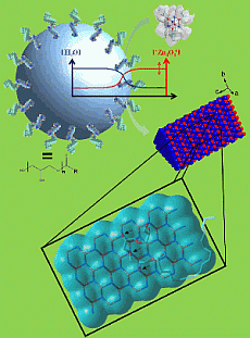
|
|
(24) Recombination dynamics in ZnO nanowires: Surfaces states versus mode quality factor
J. S. Reparaz1, F. Güell2, M. R. Wagner1, G. Callsen1, R. Kirste1, S. Claramunt2, J. R. Morante2,3 and A. Hoffmann1
1 Institute of Solid State Physics, Technische Universität Berlin, Hardenbergstr. 36, 10623 Berlin, Germany
2 M2E-IN2UB, Departament dElectrònica, Universitat de Barcelona, C/Martí i Franquès 1, Catalunya, 08028 Barcelona, Spain
3 Institut de la Recerca de lEnergia de Catalunya (IREC), C/Josep Pla 2, 08019 Barcelona, Catalunya, Spain
|
In this work, we investigate the influence of finite size on the recombinations dynamics of ZnO nanowires. We demonstrate that diameter as well as length of nanowires determine the lifetime of the neutral donor bound excitons. Our findings suggest that while the length is mainly responsible for different mode quality factors of the cavity-like nanowires, the diameter determines the influence of surface states as alternative recombinations channels for the optical modes trapped in the nanocavity. In addition, comparing nanowires grown using different catalyst we show that the surfaces states strongly depend on each precursor characteristics.
Applied Physics Letters 97, 133116 (Oct. 01, 2010)
|
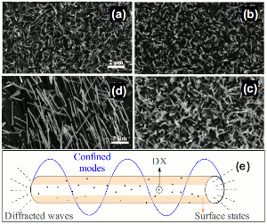
|
|
(23) Excited state properties of donor bound excitons in ZnO
B. K. Meyer1, J. Sann1, S. Eisermann, S. Lautenschläger1, M. R. Wagner2, M. Kaiser, G. Callsen, J. S. Reparaz, and A. Hoffmann2
1 I. Physikalisches Institut, Justus-Liebig-Universität Gießen, Heinrich-Buff-Ring 16, 35392 Gießen, Germany
2 Institute of Solid State Physics, Technische Universität Berlin, Hardenbergstr. 36, 10623 Berlin, Germany
|
ZnO shows a great variety of richly structured luminescence lines in a very narrow energy range of 30 meV below the free A-exciton line. At very low temperatures the majority of these lines can be explained by radiative recombination of excitons bound to neutral and ionized donors. With increasing temperature even more photoluminescence (PL) lines appear with activation energies which indicate the involvement of excited states of the bound exciton complexes. Based on high-resolution temperature-dependent luminescence and luminescence excitation experiments we investigate the excited states properties of donor bound excitons in ZnO. Several possible configurations of excited states could be distinguished: (i) excitons which involve a hole from the B- instead of the A-valence band, (ii) vibrational-rotational excited states of the excitons, and (iii) electronic excited states of the excitons. Magneto-PL measurements of the ground and vibrational-rotational excited states corroborate the identification of the excited states with comparable g-factors for all shallow donor bound excitons. In addition to the excited states, energy transfer processes via the ionized bound excitons and free exciton polaritons are observed. The experimental results are supported by theoretical calculations and demonstrate that ZnO is a unique compound semiconductor where the basics of atomic and molecular physics can be studied and understood in a solid state matrix.
Physical Review B 82, 115207 (Sep. 14, 2010)
|
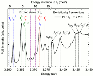
|
|
(22) Optical properties of InN grown on templates with controlled surface polarities
R. Kirste1, M. R. Wagner1, J.-H. Schulze1, A. Strittmatter1, R. Collazo2, Z. Sitar2, M. Alevli3, N. Dietz3, and A. Hoffmann1
1 Institute of Solid State Physics, Technical University Berlin, Hardenbergstrasse 36, 10623 Berlin, Germany
2 Department of Materials Science and Engineering, North Carolina State University, 1210 Varsity Dr, 27606 Raleigh, NC, USA
3 Physics and Astronomy Department, Georgia State University, 29 Peachtree Center Avenue, 30303-4106 Atlanta, GA, USA
|
The structural and optical properties of InN layers grown on GaN/sapphire templates with controlled Ga-/N-polar surfaces are investigated. Raman spectroscopy and XRD reciprocal space map analysis suggest that the InN layers were grown strain free with a high crystal quality. A line shape analysis of the A1(LO) Raman mode yields to a decreasing carrier concentration for the sample grown on Ga-polar substrate. Low temperature photoluminescence measurements exhibit a shift to lower energies of the luminescence maximum for the sample grown on Ga-polar GaN probably due to a reduced carrier concentration and thus, a decreased Burstein-Moss shift. Following this, we demonstrate that the use of polarity controlled GaN/sapphire substrates leads to unstrained layers with good structural and optical properties.
Physica Status Solidi B 207, 2351 (Jul. 09, 2010)
|
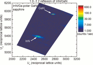
|
|
(21) A molecular precursor route to a metastable form of zinc oxide
C. L. Pueyo1, S. Siroky1, S. Landsmann1, M. W. E. van den Berg2, M. R. Wagner3, J. S. Reparaz3, A. Hoffmann3, and S. Polarz1
1 Department for Chemistry, University of Konstanz, D-78457 Konstanz, Germany
2 Tronox Pigments GmbH, Rheinuferstrasse 7-9, D-47829 Krefeld, Germany
3 Institute of Solid State Physics, Technical University Berlin, Hardenbergstrasse 36, 10623 Berlin, Germany
|
Important changes in properties are observed in many instances when at constant composition materials possessing different crystal structure, so-called polymorphs are considered. Because many viable polymorphs have not yet been realized experimentally, it is an important task to learn about the factors which determine the formation of metastable phases. The preparation of such phases is particularly challenging when the thermodynamically stable phase forms already under mild conditions. Zinc oxide with Wurtzite structure represents such a case and due to its multifunctional character it is currently in the focus of research in many areas. Thus, it can be envisioned that zinc oxide materials with a structure different to Wurtzite will exhibit new, exciting and eventually unforeseeable properties. The preparation of ZnO under kinetically controlled conditions using an organometallic precursor system is presented here. The formation of a new, nanocrystalline phase with 99% purity has been observed at low temperatures (T = 2°C). The analysis of the new phase with a variety of analytical methods including PXRD, DSC, XANES/ EXAFS, HRTEM, FT-Raman and optical spectroscopy leads to the conclusion that a metastable ZnO with a crystal structure resembling the alpha-boron nitride structure has been prepared. The formation of this material represents a novel example for the application of the Ostwald step-rule in materials science.
Chemistry of Materials 22, 4263 (Jun. 18, 2010)
|
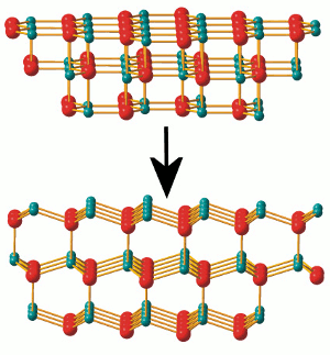
|
|
(20) Reduction of the transverse effective charge of optical phonons in ZnO under pressure
J. S. Reparaz1, L. R. Muniz2, M. R. Wagner1, A. R. Goñi2, M. I. Alonso2, A. Hoffmann1, and B. K. Meyer3
1 Institute of Solid State Physics, Technische Universität Berlin, Hardenbergstr. 36, 10623 Berlin, Germany
2 Institut de Ciència de Materials de Barcelona CSIC, Esfera UAB, 08193 Bellaterra, Spain
3 I. Physikalisches Institut, Justus-Liebig-Universität Gießen, Heinrich-Buff-Ring 16, 35392 Gießen, Germany
|
From Raman scattering on a-plane wurtzite ZnO crystals we obtained a decreasing splitting between longitudinal and transversal optical phonons with A1 and E1 symmetry as a function of hydrostatic pressure up to 5.5 GPa. Consequently, the transverse effective charge (eT*) exhibits a strong reduction with increasing pressure, yielding 2.1714.6×10-3 P/GPa and 2.0413.7×10-3 P/GPa (in units of the elementary charge) for the A1 and E1 phonons, respectively. We find a clear systematic in the linear pressure coefficient of eT* with bond polarity for the series of wide-band gap semiconductors SiC, AlN, GaN, and ZnO.
Applied Physics Letters 96, 231906 (Jun. 09, 2010)
|
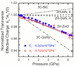
|
|
(19) ClebschGordan coefficients for scattering tensors in ZnO and other wurtzite semiconductors
H. W. Kunert1, M. R. Wagner2, A. G. J. Machatine1, P. Niyongabo1, J. B. Malherbe1, A. Hoffmann2, J. Barnas3, and W. Florek3
1 Department of Physics, University of Pretoria, 0002, South Africa
2 Institute of Solid State Physics, Technische Universität Berlin, Hardenbergstr. 36, 10623 Berlin, Germany
3 Department of Physics, Adam Mickiewicz University, ul. Ulmutowska 85, 61-614 Poznan, Poland
|
Selection rules for inter- and intra-valley scattering processes between the minima of the lowest conduction band Gamma, L, M, and A are investigated in wurtzite ZnO. The knowledge of the selection rules is required for the determination of the Clebsch-Gordon coefficients (CGCs). These coefficients diagonalize the Kronecker products (KPs) of relevant irreducible representations of quasi particles participating in scattering processes. The elements of the scattering tensors are the linear combinations of the CGCs. Within this work, the CGCs for ZnO belonging to the space group are determined.
Physica Status Solidi B 247, 1802 (May. 17, 2010)
|
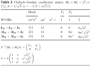
|
|
(18) Identification of a donor-related recombination channel in ZnO thin films
M. Brandt1, H. v. Wenckstern1, G. Benndorf1, M. Lange1, C. P. Dietrich1, C. Kranert1, C. Sturm1, R. SchmidtGrund1, H. Hochmuth1, M. Lorenz1, M. Grundmann1, M. R. Wagner2, M. Alic2, C. Nenstiel2, and A. Hoffmann2
1 Institut für Experimentelle Physik II, Universität Leipzig, Linnèstr. 5, 04103 Leipzig, Germany
2 Institute of Solid State Physics, Technische Universität Berlin, Hardenbergstr. 36, 10623 Berlin, Germany
|
An excitonic recombination line is observed in photoluminescence spectra of ZnO thin films at 3.3465 eV. The line is labeled I12. Its appearance was only observed in samples grown on a MgO or heavily aluminumdoped ZnO buffer layer. The properties of the recombination mechanism were probed by photoluminescence and photoluminescence-excitation spectroscopy. The recombination was classified to be an exciton bound to a neutral donor. Both an ionized state and a two-electron satellite transition were observed and could be correlated with the central transition. The excitation channels are similar to those of the well-known I6 transition related to AlZn. The localization energy was calculated to be 29.4 meV. A donor activation energy of 90.8 meV was extrapolated using the Haynes rule for ZnO.
Physical Review B 81, 073306 (Feb. 26, 2010)
|
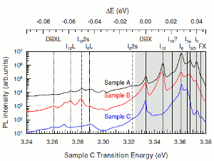
|
|
(17) Size-dependent recombination dynamics in ZnO nanowires
J. S. Reparaz1, F. Güell2, M. R. Wagner1, A. Hoffmann1, A. Cornet, 3, and J. R. Morante2,4
1 Institut für Festkörperphysik, Technische Universität Berlin, Hardenbergstr. 36, 10623 Berlin, Germany
2 M2E-IN2UB, Departament dElectrònica, Universitat de Barcelona, C/Martí i Franquès 1, Catalunya, 08028 Barcelona, Spain
3 MIND-IN2UB, Departament dElectrònica, Universitat de Barcelona, C/Martí i Franquès 1, Catalunya, 08028 Barcelona, Spain
4 Institut de la Recerca de lEnergia de Catalunya (IREC), C/Josep Pla 2, 08019 Barcelona, Catalunya, Spain
|
A deep understanding of the recombination dynamics of ZnO nanowires (NWs) is a natural step for a precise design of on-demand nanostructures based on this material system. In this work we investigate the influence of finite-size on the recombination dynamics of the neutral bound exciton around 3.365 eV for ZnO NWs with different diameters. We demonstrate that the lifetime of this excitonic transition decreases with increasing the surface-to-volume ratio due to a surface induced recombination process. Furthermore, we have observed two broad transitions around 3.341 and 3.314 eV, which were identified as surface states by studying the dependence of their life time and intensitiy with the NWs dimensions.
Applied Physics Letters 96, 053105 (Feb. 01, 2010)
|
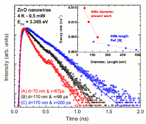
|
|
(16) Lithium related deep and shallow acceptors in Li-doped ZnO nanocrystals
C. Rauch1, W. Gehlhoff1, M. R. Wagner1, E. Malguth1, G. Callsen1, R. Kirste1, B. Salameh1,2, A. Hoffmann1, S. Polarz3, Y. Aksu4, and M. Driess4
1 Institut für Festkörperphysik, Technische Universität Berlin, Hardenbergstr. 36, 10623 Berlin, Germany
2 Department of Applied Physics, Tafila Technical University, Tafila 66110, Jordan
3 Department of Chemistry, University of Konstanz, D-78457 Konstanz, Germany
4 Institute of Chemistry, Metalorganics and Inorganic Materials, TU Berlin, Straße des 17. Juni 135, D-10623 Berlin, Germany
|
We study the existence of Li-related shallow and deep acceptor levels in Li-doped ZnO nanocrystals
using electron paramagnetic resonance (EPR) and photoluminescence (PL) spectroscopy. ZnO nanocrystals with adjustable Li concentrations between 0% and 12% have been prepared using organometallic precursors and show a significant lowering of the Fermi energy upon doping. The deep Li acceptor with an acceptor energy of 800 meV could be identified in both EPR and PL measurements and is responsible for the yellow luminescence at 2.2 eV. Additionally, a shallow acceptor state at 150 meV above the valence band maximum is made responsible for the observed donor-acceptor pair and free electron-acceptor transitions at 3.235 and 3.301 eV, possibly stemming from the formation of Li-related defect complexes acting as acceptors.
Journal of Applied Physics 107, 024311 (Jan. 27, 2010)
|
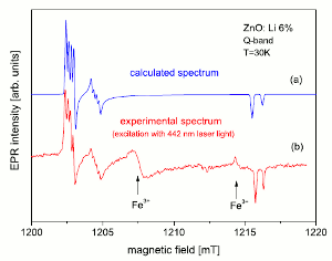
|
|
(15) Polariton effects in the dielectric function of ZnO excitons obtained
by ellipsometry
M. Cobet1, C. Cobet2, M. R. Wagner1, N. Esser2, C. Thomsen1, and A. Hoffmann1
1 Institut für Festkörperphysik, Technische Universität Berlin, Hardenbergstr. 36, 10623 Berlin, Germany
2 ISAS-Institute for Analytical Sciences, 12489 Berlin, Germany
|
The complex dielectric tensor of ZnO in the regime of the excitonic transitions is determined with ellipsometry and analyzed concerning the quantization of the electromagnetic field in terms of
coupled polariton-eigenmodes. Negative sections in the real part indicate the significant formation of polaritons for the dipole-allowed excitons of the Gamma 7, Gamma 9, Gamma 7. The transverse-longitudinal splittings which separate the upper polariton branch from the lower branch, corresponding to the k-vector of the used light, are deduced precisely for each subband. Mainly for E parallel c, additional absorption peaks are observed at the longitudinal B-exciton and closely above. One is considered to be a mixed-mode and the other is seen as a consequence of interference effects in an exciton free surface layer which is also visible in reflectance anisotropy spectroscopy.
Applied Physics Letters 96, 031905 (Jan. 19, 2010)
|
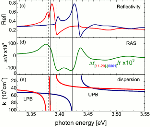
|
|
2009
(14) Gamma 7 valence band symmetry related hole fine splitting of bound excitons in ZnO observed in magneto-optical studies (Editor's Choice)
M. R. Wagner1, J.-H. Schulze1, R. Kirste1, M. Cobet1, A. Hoffmann1, C. Rauch2, A. Rodina3, B. K. Meyer4, U. Röder5, and K. Thonke5
1 Institut für Festkörperphysik, Technische Universität Berlin, Hardenbergstr. 36, 10623 Berlin, Germany
2 Department of Applied Physics, Helsinki University of Technology, P.O. Box 1100, Helsinki FIN-02015 TKK, Finland
3 A. F. Ioffe Physico-Technical Institute, 194021 St. Petersburg, Russia
4 I. Physikalisches Institut, Justus-Liebig-Universität Gießen, Heinrich-Buff-Ring 16, 35392 Gießen, Germany
5 Institut für Halbleiterphysik, Universität Ulm, Albert-Einstein-Allee 45, 89081 Ulm, Germany
|
The symmetry ordering of the valence bands in ZnO is derived from high-resolution magneto-optical measurements of bound excitons. We report on the experimental observation of a hole state related fine splitting for bound excitons in the Voigt configuration. This splitting is related to a nonzero Landé g value for hole states from the A valence band. Based on theoretical considerations, the symmetry of the uppermost valence band is doubtlessly identified as Gamma 7. This attribution is confirmed by polarization and angular resolved magnetophotoluminescence spectroscopy.
Physical Review B 80, 205203 (Nov. 18, 2009)
|
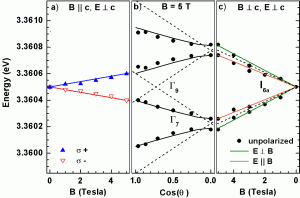
|
|
(13) A systematic study on zinc oxide materials containing group I metals (Li, Na, K)-synthesis from organometallic precursors, characterization, and properties
S. Polarz1, A. Orlov1, A. Hoffmann2, M. R. Wagner2, C. Rauch2, R. Kirste2, W. Gehlhoff2, Y. Aksu3, M. Driess3, M. W. E. van den Berg4 and M. Lehmann5
1 Department for Chemistry, University of Konstanz, D-78457 Konstanz, Germany
2 Institute of Solid-State Physics, Technical University Berlin, Hardenbergstrasse 36, 10623 Berlin, Germany
3 Institute of Chemistry, Technical University Berlin, Straße des 17. Juni 135, 10623 Berlin, Germany
4 Department for Chemistry, Ruhr-Universitaet Bochum, Universitaetsstrasse 150, 44780 Bochum, Germany
5 Institute for Optics and Atomic Physics, Technical University Berlin, Straße des 17. Juni 135, 10623 Berlin, Germany
|
The reproducible preparation of p-type ZnO represents an important task that might be realized via the partial substitution of Zn2+ by Li+ in the ZnO lattice. Consequently, it is necessary to understand the effect of Li incorporation into ZnO in detail. A systematic approach employing molecular organometallic precursors for the preparation of ZnO materials containing different amounts of Li is presented. The materials have been characterized with various analytical techniques including X-ray absorption, micro-Raman, and low-temperature photoluminescence spectroscopy; high-resolution transmission electron microscopy; powder X-ray diffraction; and electron paramagnetic resonance. It could be seen that Li incorporation is successful only below 12% Li. Already at 1% Li, a maximum in lattice substitution seems to be reached. At higher Li contents, more and more interstitial sites become occupied.
Chemistry of Materials 21, 3889 (Aug. 04, 2009)
|
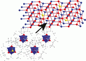
|
|
(12) Influence of substrate surface polarity on homoepitaxial growth of ZnO layers by chemical vapor deposition
M. R. Wagner1, T. P. Bartel1, R. Kirste1, A. Hoffmann1, J. Sann2, S. Lautenschläger2, B. K. Meyer2 and C. Kisielowski3
1 Institut für Festkörperphysik, Technische Universität Berlin, Hardenbergstr. 36, 10623 Berlin, Germany
2 I. Physikalisches Institut, Justus-Liebig-Universität Gießen, Heinrich-Buff-Ring 16, 35392 Gießen, Germany
3 National Center for Electron Microscopy, Lawrence Berkeley National Laboratory, 1 Cyclotron Road, Berkeley, CA 94720, USA
|
The influence of the substrate polarity (Zn-polar or O-polar) on the structural and optical properties of homoepitaxial ZnO epilayers grown by chemical vapor deposition is investigated. The polarity of the epilayer is controlled by the substrate polarity as shown by high resolution TEM imaging. Changes in stoichiometry in the epilayer are studied by quantitative TEM analysis. A small compressive strain of ecc=3·10-4 is observed in both epilayers and XRD measurements indicate a superior structural quality of the epilayers compared to the substrate. Cross-sectional Raman spectroscopy also demonstrates the superior quality of the epilayers, although high strain is present within the substrates. The phonon deformation potential parameters of the strain sensitive E2(high) Raman mode are determined to a=-730cm-1 and b=-1000cm-1. Differences in the excitonic luminescence including the appearance of new emission lines and an increased full width at half maximum in O-face epilayers are observed. It is suggested that the impurity diffusion from the substrate to the layer is affected by the substrate surface polarity with lower impurity concentrations in the Zn-polar film, compared to the O-polar epilayer.
Physical Review B 79, 035307 (Jan. 09, 2009)
|
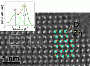
|
|
2008
(11) Nitrogen incorporation in homoepitaxial ZnO CVD epilayers
S. Lautenschläger1, S. Eisermann1, B. K. Meyer1, G. Callsen2, M. R. Wagner2, and A. Hoffmann2
1 I. Physikalisches Institut, Justus-Liebig-Universität Gießen, Heinrich-Buff-Ring 16, 35392 Gießen, Germany
2 Institut für Festkörperphysik, Technische Universität Berlin, Hardenbergstr. 36, 10623 Berlin, Germany
|
ZnO:N thin films have been deposited on oxygen and zinc terminated polar surfaces of ZnO. The nitrogen incorporation in the epilayers, using NH3 as doping source, was investigated as a function of the growth temperature in the range between 380°C and 580°C. We used Raman spectroscopy and low temperature photoluminescence to investigate the doping properties. It turned out that the nitrogen incorporation strongly depends on both, the surface polarity of the epitaxial films and the applied growth temperatures. In our CVD process low growth temperatures and Zn-terminated substrate surfaces clearly favour the nitrogen incorporation in the ZnO thin films.
Physica Status Solidi RRL 3, 16 (Nov. 07, 2008)
|
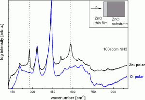
|
|
(10) Bound and free excitons in ZnO. Optical selection rules in the absence and presence of time reversal symmetry
M. R. Wagner1, H. W. Kunert2, A. G. J. Machatine2, A. Hoffmann1, P. Niyongabo2, J. Malherbe2, and J. Barnas3
1 Institut für Festkörperphysik, Technische Universität Berlin, Hardenbergstr. 36, 10623 Berlin, Germany
2 Department of Physics, University of Pretoria, 0002, South Africa
3 Department of Physics, Adam Mickiewicz University, ul. Ulmutowska 85, 61-614 Poznan, Poland
|
The correlation between ionized donor bound exciton recombinations and neutral donor bound exciton recombinations in ZnO has been investigated. The experimental data obtained by means of magneto-photoluminescence (MPL) concerning charge state and localization energies of ionized and neutral donor bound excitons are in good agreement with theoretical predictions. The optical selection rules in absence and presence of time reversal symmetry (TRS) are investigated. It is shown that the inclusion of extra degeneracy due to TRS reveals a number of new states of the same symmetries and essentially does not change the existing optical selection rules.
Microelectronics Journal 40, 289 (Sept. 24, 2008)
|
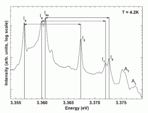
|
|
(09) Elementary excitations in Si, Ge, and diamond time reversal affected
H. W. Kunert1, A. G. J. Machatine1, J. B. Malherbe1, J. Barnas2, A. Hoffmann3, M. R. Wagner3
1 Department of Physics, University of Pretoria, 0002, South Africa
2 Department of Physics, Adam Mickiewicz University, ul. Ulmutowska 85, 61-614 Poznan, Poland
3 Institut für Festkörperphysik, Technische Universität Berlin, Hardenbergstr. 36, 10623 Berlin, Germany
|
The Space Symmetry and the Time Reversal Symmetry of vibrational modes in Si, Ge and diamond are investigated. Using Space Symmetry we have derived the Lattice Mode Representation. Reducing it onto phonon species we obtain the symmetry allowed phonons and their degeneracies. Using reality test for irreducible representations according to those the phonons are classified we determine which modes are Time Reversal affected. Comparison with experimental data obtained by neutron scattering is made. The effect of Time Reversal Symmetry on electrons in the conduction band and holes in the valence band as well as on excitons is briefly discussed.
Thin Solid Films 517, 372 (Aug. 16, 2008)
|
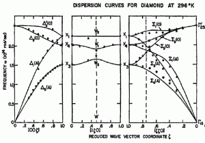
|
|
(08) Infrared absorption, multiphonon processes and time reversal effect on Si and Ge band structure
H. W. Kunert1, A. G. J. Machatine1, J. B. Malherbe1, J. Barnas2, A. Hoffmann3, M. R. Wagner3
1 Department of Physics, University of Pretoria, 0002, South Africa
2 Department of Physics, Adam Mickiewicz University, ul. Ulmutowska 85, 61-614 Poznan, Poland
3 Institut für Festkörperphysik, Technische Universität Berlin, Hardenbergstr. 36, 10623 Berlin, Germany
|
We have examined the effect of Time Reversal Symmetry (TRS) on vibrational modes and on the electronic
band structure of Si and Ge. Most of the primary non-interacting modes are not affected by TRS. Only
phonons originating from high symmetry lines S and A of the Brillouin Zone (BZ) indicate extra degeneracy.
Selection rules for some two and three phonons originating from high symmetry lines are determined. The
states of electrons and holes described by electronic band structure due to spin-inclusion are assigned by
spinor representations of the double space group. Inclusion of the TRS into the band structure results in extra
degeneracy of electrons and holes, and therefore optical selection rules suppose to be modified.
Thin Solid Films 517, 134 (Aug. 16, 2008)
|
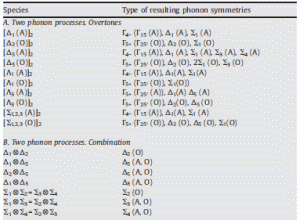
|
|
(07) Asymmetry in the excitonic recombinations and impurity incorporation of the two polar faces of homoepitaxially grown ZnO films
S. Lautenschlaeger1, J. Sann1, N. Volbers1, B. K. Meyer1, A. Hoffmann2, U. Haboeck2, and M. R. Wagner2
1 I. Physikalisches Institut, Justus-Liebig-Universität Gießen, Heinrich-Buff-Ring 16, 35392 Gießen, Germany
2 Institut für Festkörperphysik, Technische Universität Berlin, Hardenbergstr. 36, 10623 Berlin, Germany
|
Homoepitaxial ZnO layers were grown on O-polar and Zn-polar surfaces of ZnO single crystal substrates by chemical vapor deposition. While the structural properties (surface roughness and rocking curve half width) were identical within experimental error, the optical properties as monitored by photoluminescence (PL) were strikingly different. Four excitonic recombination lines are exclusively found on the O-polar surface. In order to understand the defects involved, secondary ion mass spectrometry was employed which clearly demonstrated that the impurity incorporation is substantially higher on the O-polar surface. Temperature and power dependent PL measurements provide further insight into the initial-final state recombinations. The observed recombinations are caused by excitons bound to a neutral defect complex. In order to account for the thermalization behavior found in the temperature dependent measurements, splittings in the excited as well as in the ground state must be present. Possible defect models are discussed.
Physical Review B 77, 144108 (Apr. 10, 2008)
|
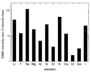
|
|
(06) Optical and structural properties of homoepitaxial ZnO
T. P. Bartel1, M. R. Wagner1, U. Haboeck1, A. Hoffmann1, C. Neumann2, S. Lautenschläger2, J. Sann2, and B. K. Meyer2
1 Institut für Festkörperphysik, Technische Universität Berlin, Hardenbergstr. 36, 10623 Berlin, Germany
2 I. Physikalisches Institut, Justus-Liebig-Universität Gießen, Heinrich-Buff-Ring 16, 35392 Gießen, Germany
|
Two dimensional homoepitaxial growth of high quality ZnO epilayers was achieved by chemical vapor deposition techniques without a buffer layer. We report on the optical and structural properties of these epilayers with particular focus on the polarity of the surface of the substrate. Photoluminescence spectra exhibit strong dependence of the bound exciton recombinations on the termination of the substrate. This is particularly pronounced in the large variety of transition lines in the O-face terminated sample with values for the full width at half maximum as low as 80µeV. Cross-sectional micro Raman spectroscopy and high resolution transmission electron microscopy reveal the presence of strain in the epilayer grown on O-face ZnO by a shift of the non-polar E2(high) mode and a variation in the lattice constant ratio. Still, the crystal quality of the films is further increased compared to the substrate, which is shown be a half-width of 17" of the XRD rocking curve in both epilayers on Zn-face and O-face terminated ZnO substrate.
Proceedings of SPIE - Zinc Oxide Materials and Devices III - Vol. 6895, F. H. Teherani, C. W. Litton, Editors, 689502 (Feb. 15, 2008)
|
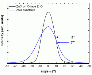
|
|
2007
(05) Phonons and electronic states of ZnO, Al2O3 and Ge in the presence of time reversal symmetry
A. G. J. Machatine1, H. W. Kunert1, A. Hoffmann2, J. B. Malherbe1, J. Barnas3, R. Seguin2, M. R. Wagner2, P. Niyongabo1, and N. Nephale1
1 Department of Physics, University of Pretoria, 0001 Pretoria, South Africa
2 Institut für Festkörperphysik, Technische Universität Berlin, Hardenbergstr. 36, 10623 Berlin, Germany
3 Department of Physics, Adam Mickiewicz University, Poznan, Poland
|
Using group theoretical techniques we have investigated all single valued representations as well as double valued, these follow from the inclusion of spin, of wurtzite (e.g. ZnO), trigonal (e.g. Al2O3) and cubic (e.g. Ge) structures, with the C6v4, D3d6 and Oh7 space groups, respectively, with regard to the presence or absence of Time Reversal Symmerty (TRS). We have found a number of phonons in wurtzite and trigonal structures to be time reversal degenerate, whereas in the cubic Si, Ge and diamond the vibrational modes are not time reversal degenerate. Electronic band structure also experience extra TRS degeneracy. Therefore, the selections rules for optical radiative transitions need modification.
Journal of Physics: Conference Series 92, 012071 (Dec. 2007)
|
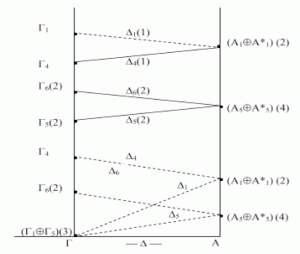
|
|
(04) Ionized and neutral donor-bound excitons in ZnO
B. K. Meyer1, J. Sann1, S. Lautenschläger1, M. R. Wagner2, and A. Hoffmann2
1 I. Physikalisches Institut, Justus-Liebig-Universität Gießen, Heinrich-Buff-Ring 16, 35392 Gießen, Germany
2 Institut für Festkörperphysik, Technische Universität Berlin, Hardenbergstr. 36, 10623 Berlin, Germany
|
We show for ZnO a correlation between the ionized donor bound exciton D+X recombinations I0, I1, and I2 and the neutral donor bound exciton D0X recombinations I6a, I8, and I9, respectively. The experimental data on the localization energies of ionized and neutral donor bound excitons are compared to theoretical predictions and a good agreement is found. We give an estimate of the localization energies of neutral acceptor bound excitons. One can conclude that the localization energies of neutral donor and acceptor bound excitons in ZnO will be very close in energy and an assignment of transition lines to donors and/or acceptors (in the absence of decisive data from magneto-optics) will not be straightforward.
Physical Review B 76, 184120 (Nov. 28, 2007)
|
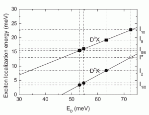
|
|
(03) Resonant Raman scattering at exciton intermediate states in ZnO
M. R. Wagner1, P. Zimmer1, A. Hoffmann1, C. Thomsen1
1 Institut für Festkörperphysik, Technische Universität Berlin, Hardenbergstr. 36, 10623 Berlin, Germany
|
We present results on resonant Raman scattering in single crystal ZnO using a continuously tuneable excitation in the energy region of the free and bound excitons. The PL and Raman spectra show the presence of a dominant luminescence band at 3.310 eV as well as the A1(TO), E2(high), E1(LO), and 2E1(LO) Raman modes at liquid nitrogen temperature. A strong resonance of the Raman scattering cross section was found for the second-order 2E1(LO) phonon mode. This enhancement is considerably larger than for the non-polar E2(high) mode due to Fröhlich interaction. Furthermore, the resonance enhancement at bound excitons was studied at liquid helium temperature proving the essential role of excitonic intermediate states for resonant Raman scattering in ZnO.
Physica Status Solidi RRL 1, 169 (Jul. 03, 2007)
|
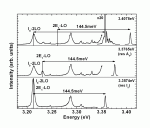
|
|
(02) Photonic properties of ZnO epilayers
M. R. Wagner1, U. Haboeck1, P. Zimmer1, A. Hoffmann1, S. Lautenschläger2, J. Sann2, and B. K. Meyer2
1 Institut für Festkörperphysik, Technische Universität Berlin, Hardenbergstr. 36, 10623 Berlin, Germany
2 I. Physikalisches Institut, Justus-Liebig-Universität Gießen, Heinrich-Buff-Ring 16, 35392 Gießen, Germany
|
The characterization by various experimental techniques of homoepitaxial growth and photonic properties of ZnO epilayers was exhaustively analyzed. The photonic properties of ZnO as promising material for the realization of polariton lasers were investigated by angular dependent reflection spectroscopy. The fitting of the polariton dispersion curve with the experimental results provided us information about the longitudinal-transverse exciton-polariton splitting and damping constants. In addition, the valence band symmetry was examined by angular resolved magneto-optical photoluminescence. From our theoretical and experimental results we extracted evidence that the topmost A valence band possesses Gamma7 symmetry. Micro-Raman spectroscopy revealed even in homoepitaxially grown samples the existence of compressive or tensile strain which varied not only in the ZnO layers but also in the templates. In contrast, the untreated substrates were uniformly strained. Sporadically crystal perturbations culminating in the formation of separated growth domains were observed. Additionally, resonant Raman scattering was performed, showing a strong enhancement of the 2E1(LO) mode for resonant excitation of the I8 bound exciton complex. We suggest that the resonant Raman scattering led to a longer lifetime of the resonantly excited phonon mode due to a strong exciton-phonon interaction.
Proceedings of SPIE - Zinc Oxide Materials and Devices II - Vol. 6474, F. H. Teherani, C. W. Litton, Editors, 64740X (Feb. 20, 2007)
|
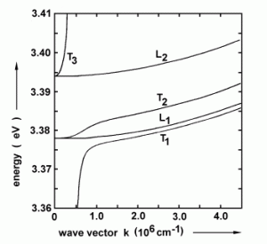
|
|
2006
(01) Phonons in sapphire Al2O3 substrate for ZnO and GaN
H. W. Kunert1,2, A. G. J. Machatine2, A. Hoffmann1, G. Kaczmarczyka1, U. Haboeck1, J. B. Malherbe2, J. Barnas3, M. R. Wagner1, and J. D. Brink2
1 Institut für Festkörperphysik, Technische Universität Berlin, Hardenbergstr. 36, 10623 Berlin, Germany
2 Department of Physics, University of Pretoria, 0001 Pretoria, South Africa
3 Department of Physics, Adam Mickiewicz University, Poznan, Poland
|
By means of standard method of placing the vectors upon each ion in the basis (2-Al, 3-O) and acting by symmetry operators of sapphire space group onto the basis we obtain Lattice Mode Representation (LMR). The decomposition of the LMR onto irreducible representations (irrps) corresponding to the high symmetry point and lines results in symmetry allowed first order non-interacting modes originating from the entire first Brilloiun zone. First order Raman active modes are determined by symmetrized square of Kronecker products of sapphire vector representation. The selection rules for the second and third order Raman processes follow from the symmetrized Kronecker Products (square and cubes). Frequently the irrps are complex. In such cases the time reversal symmetry (TRS) must be taken into account. We have also investigated the effect of the TRS in sapphire and ZnO which leads to an extra degeneracy.
Materials Science and Engineering C 27, 1222 (Oct. 05, 2006)
|
|
|
|
|